Multi-color display apparatus

a multi-color display and apparatus technology, applied in the direction of discharge tube luminescnet screen, discharge tube/lamp details, organic semiconductor device, etc., can solve the problems of reducing the internal quantum efficiency, and reducing the light-extraction efficiency, so as to improve the apparent deterioration of a durable luminance, and improve the light-extraction efficiency

Inactive Publication Date: 2009-05-07
CANON KK
View PDF4 Cites 5 Cited by
  • Summary
  • Abstract
  • Description
  • Claims
  • Application Information

AI Technical Summary

Benefits of technology

[0012]According to the present invention, light-extraction efficiency is gradually improved by current flow. Therefore, the improvement of light-extraction efficiency is balanced with the reduction of an internal quantum efficiency due to the current flow, so that apparent deterioration of a durable luminance can be almost eliminated. Then, the present invention exerts an excellent effect that a multi-color display apparatus having little burn-in can be provided.

Problems solved by technology

However, the reduction of the light-extraction efficiency which is caused by change in a light-emitting region with the elapse of time as well as a measure to avoid the reduction are not known at all.
That is, even when the light-extraction efficiency is improved by the interference effect, a light-emitting device made of a conventionally known organic material has a problem that the internal quantum efficiency is gradually reduced by current flow, or the light-emitting region is gradually changed to reduce the light-extraction efficiency.
Therefore, there is a problem that the durability for stable light emission reduces.
Then, when the device is used to produce a display apparatus, there is a problem that burn-in occurs.

Method used


Image

  • Multi-color display apparatus
  • Multi-color display apparatus
  • Multi-color display apparatus

Examples


example 1

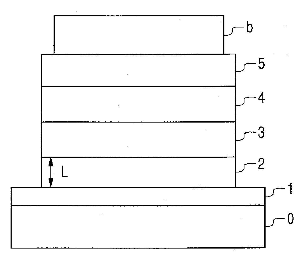
[0057]Example 1 and Comparative Example 1 show a manufacturing procedure of a multi-color display apparatus using the organic light-emitting devices each having the top-emission structure as shown in FIG. 2 in which the reflection electrode is made of Cr, and measured device characteristics thereof.

[0058]A substrate obtained by forming TFTs, circuits, Cr anodes (reflection electrodes), a planarizing film, a device isolation film, and the like on a glass and provided with an electrode for multi-color display which is capable of performing 200-ppi display (reference numerals 10 and 11 in FIG. 2) was subjected to UV / ozone cleaning.

[0059]Subsequently, the cleaned substrate and materials were set in a vacuum vapor deposition apparatus (produced by ULVAC KIKO, Inc.) and the vacuum vapor deposition apparatus was evacuated to 1×10⁻⁶ Torr. After that, N,N′-α-dinaphthyl-benzidine (α-NPD) was deposited on the reflection electrode 10 to form the hole transport layer 12 with a film thickness of ...

example 2

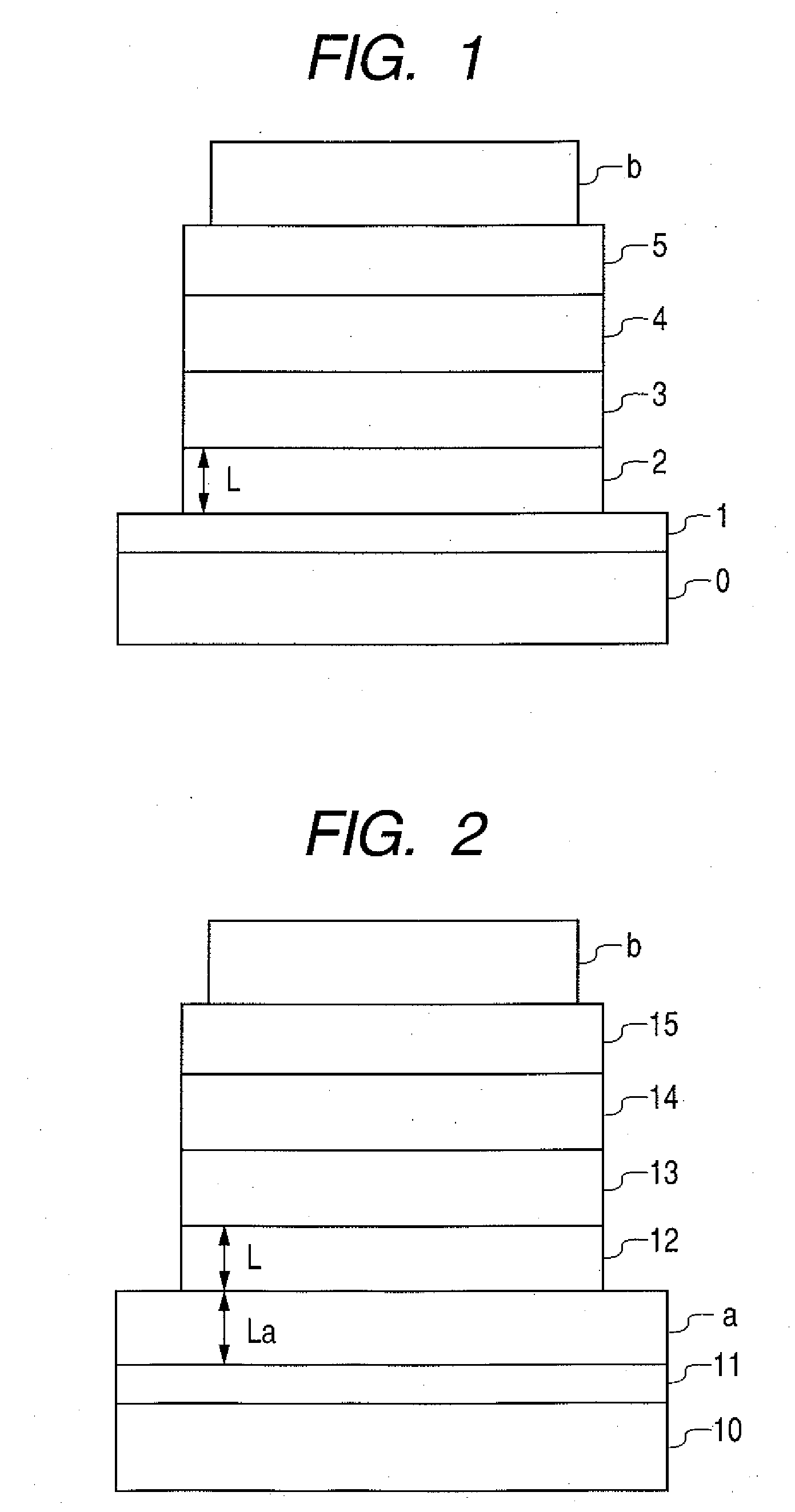
[0084]Example 2 and Comparative Example 2 show a manufacturing procedure of a multi-color display apparatus using the organic light-emitting devices each having the top-emission structure as shown in FIG. 3 in which the reflection layer is made of Ag and the transparent electrode “a” (anode) is made of IZO, and measured device characteristics thereof.

[0085]A substrate obtained by forming TFTs, circuits, Ag films serving as the reflection layers, IZO films (anodes) each having 20 nm serving as the transparent electrodes “a”, a planarizing film, a device isolation film, and the like on a glass and provide with an electrode for multi-color display which is capable of performing 200-ppi display (reference numerals 20 and 21 and reference symbol “a” in FIG. 3) was subjected to UV / ozone cleaning.

[0086]After that, a multi-color display apparatus was produced in the same manner as in Example 1, except that α-NPD was deposited to form the hole transport layer 22 with a film thickness of 10 n...

example 3

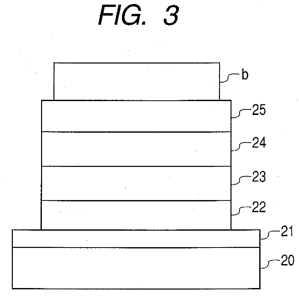
[0105]Example 3 and Comparative Example 3 show a manufacturing procedure of a multi-color display apparatus using the organic light-emitting devices each having the top-emission structure as shown in FIG. 3 in which an Ag thin film was used as the light extraction electrode “b” located on a light extraction side, and measured device characteristics thereof.

[0106]A multi-color display apparatus was produced in the same manner as in Example 2, except that a film of Ag with a film thickness of 30 nm was formed as the light extraction electrode “b”. The same measurement as that in Example 1 was performed.

[0107]A relationship between the film thickness of the reflection side and the wavelength is the same as that in Example 2. The film thicknesses and structures of the devices of Example 3 and the results obtained by measurement thereof are summarized in Table 1.

[0108]Although the initial light-extraction efficiency of the devices of Example 3 was not so high, the produced multi-color di...


PUM


Abstract

Provided is an organic light-emitting device having little apparent deterioration of a durable luminance. The organic light-emitting device includes a hole transport layer and a light-emitting layer which are located in a predetermined order between a reflection electrode for reflecting light and an electrode for transmitting light, the hole transport layer being in contact with the reflection electrode and made of an organic compound, and the light-emitting layer being made of an organic compound, wherein an optical film thickness L of the hole transport layer is set in a range of 0.25λ×(2n−1.7) to 0.25λ×(2n−1.3), where λ indicates an emission wavelength and n indicates a positive integer.

Description

TECHNICAL FIELD[0001]The present invention relates to an organic light-emitting device including a hole transport layer and a light-emitting layer which are stacked in a predetermined order between a reflection electrode for reflecting light and a transparent electrode for transmitting light, wherein the hole transport layer is in contact with the reflection electrode and made of an organic compound, and the light-emitting layer is made of an organic compound. In addition, the present invention relates to a multi-color display apparatus using the organic light-emitting device.BACKGROUND ART[0002]FIG. 3 is a schematic view showing an example of a stacked structure of a top-emission organic light-emitting device. As shown in FIG. 3, in the organic light-emitting device (organic electroluminescence (EL) device), layers each made of an organic compound are stacked between a reflection electrode (anode) 21 for reflecting light which is provided on a support substrate 20 and a transparent...

Claims


Application Information

Patent Timeline
Patent Type & Authority Applications(United States)
IPC IPC(8): H01L51/50
CPCH01L27/3211H01L51/0059H01L51/0062H01L51/0081H01L2251/558H01L51/5265H01L51/5271H01L2251/5315H01L51/0085H10K59/35H10K85/649H10K85/631H10K85/324H10K85/342H10K50/852H10K50/856H10K2102/3026H10K2102/351
Inventor TAKAYA, ITARUKIMURA, TOSHIHIDE
Owner CANON KK
Why Eureka
Try Eureka