Wireless communication device

a wireless communication and circuit board technology, applied in the direction of antenna details, protective material radiating elements, antennas, etc., can solve the problems of affecting the efficiency of the device, conflicting the philosophy of minimization and low-cost, and the clearance area requirement, so as to improve the performance of the wireless communication device, the layout region used on the circuit board can be minimized, and the effect of minimizing the use area

Inactive Publication Date: 2009-05-07
DELTA ELECTRONICS INC
View PDF2 Cites 13 Cited by
  • Summary
  • Abstract
  • Description
  • Claims
  • Application Information

AI Technical Summary

Benefits of technology

[0011]As mentioned above, since the antenna is disposed on the housing instead of the circuit board, the layout region used on the circuit board can be minimized. Thus, the wireless communication device can be minimized, or more additional electronic elements can be configured in the wireless communication device so as to improve the performance thereof. Comparing to the prior art, the configuration as well as the manufacturing processes of the wireless communication device remain as usual but the performance of transmitting signals can be enhanced via disposing the antenna unit on the housing. Furthermore, the manufacturing processes and the assemble procedures can be simplified so that the manufacturing time and cost can be reduced.

Problems solved by technology

However, the miniaturization of the antenna would affect the efficiency of the device apparently.
Nevertheless, the clearance area requirement is conflicted with the philosophy of minimization and low-cost.

Method used


Image

  • Wireless communication device
  • Wireless communication device
  • Wireless communication device

Examples


Embodiment Construction

[0018]The present invention will be apparent from the following detailed description, which proceeds with reference to the accompanying drawings, wherein the same references relate to the same elements.

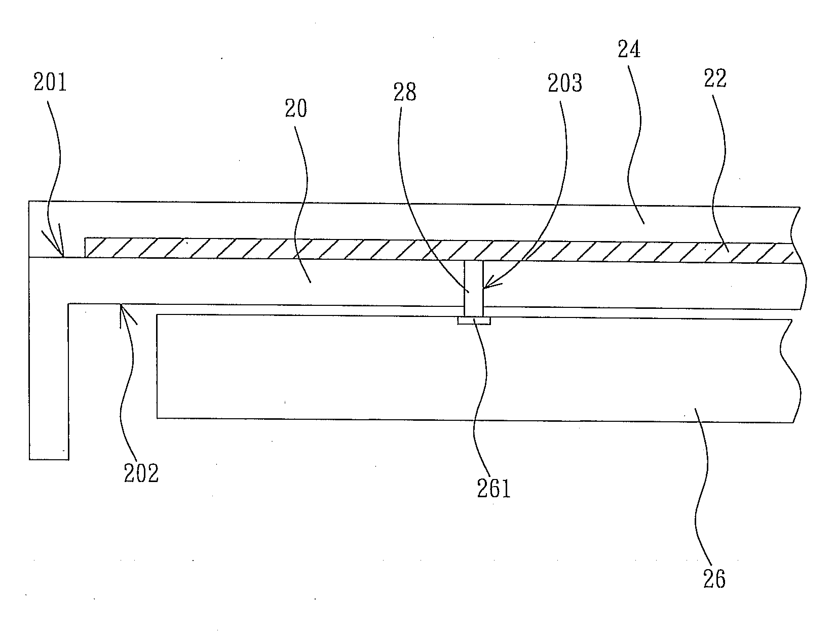
[0019]FIG. 2 is a partial cross-sectional illustration of a wireless communication device according to an embodiment of the invention. Referring to FIG. 2, the wireless communication device includes a housing 20, an antenna unit 22 and a protective layer 24. The antenna unit 22 is directly disposed on an outer surface 201 of the housing 20.

[0020]The antenna unit 22 can be electrically connected to a feeding point 261 on a circuit board 26 via a conductive wire. In the embodiment, a metal conductor 28 passes through a through hole 203 of the housing 20 to electrically connect to the feeding point 261 on the circuit board 26. The metal conductor 28 can be the above-mentioned conductive wire. The protective layer 24 covers the antenna unit 22 and at least a portion of the outer surface 2...


PUM


Abstract

A wireless communication device includes a housing and an antenna unit. The antenna unit is disposed on the outer or inner surface of the housing. A protective layer is optionally disposed to cover the outer surface of the antenna unit and, even more, at least a portion of the housing. Thus, the antenna unit separated from the circuit board does not occupy the layout region of the circuit board, so that the layout region of the circuit board can be used for other purposes. Moreover, the antenna unit formed on the housing can enhance the performance of the wireless communication device for transceiving signals.

Description

CROSS REFERENCE TO RELATED APPLICATIONS[0001]This Non-provisional application claims priority under 35 U.S.C. §119(a) on Patent Application No(s). 096141539 filed in Taiwan, Republic of China on Nov. 2, 2007, the entire contents of which are hereby incorporated by reference.BACKGROUND OF THE INVENTION[0002]1. Field of Invention[0003]The invention relates to a wireless communication device and, in particular, to a wireless communication device having metallic painted antenna.[0004]2. Related Art[0005]The wireless communication technology is continuously progressed so that various types of wireless communication electronic devices are developed. The antenna is miniaturized for achieving prettier and lighter portable wireless communication device, such as the Bluetooth earpiece, Zigbee or WiFi wireless network. However, the miniaturization of the antenna would affect the efficiency of the device apparently.[0006]FIG. 1A is a partial cross-sectional view of a wireless communication elec...

Claims


Application Information

Patent Timeline
Patent Type & Authority Applications(United States)
IPC IPC(8): H01Q1/40H01Q1/24
CPCH01Q1/40H01Q1/243
Inventor CHENG, MEI-LAN
Owner DELTA ELECTRONICS INC
Why Eureka
Try Eureka