Silicon interposer and semiconductor device package and semiconductor device incorporating the same

a technology of silicon interposer and semiconductor device, which is applied in the direction of semiconductor devices, semiconductor/solid-state device details, electrical apparatus, etc., can solve the problems of cracks at the connection sections between the wiring board and the semiconductor elements, damage to the semiconductor elements, and cracks at the connection sections to achieve the effect of reliable electrical connection

Inactive Publication Date: 2009-05-14
SHINKO ELECTRIC IND CO LTD
View PDF5 Cites 12 Cited by
  • Summary
  • Abstract
  • Description
  • Claims
  • Application Information

AI Technical Summary

Benefits of technology

[0009]To solve the problems, by providing a buffer section for relieving the thermal stress generated owing to the difference in thermal expansion coefficient between through-hole electrodes and an insulating film making contact with the through-hole electrodes, the present invention is intended to provide a silicon interposer not causing cracks between the through-hole electrodes and the insulating film making contact with the through-hole electrodes even if a thermal load is repeatedly applied to a semiconductor device having through-hole electrodes made of copper, and the present invention is also intended to provide a semiconductor device package and a semiconductor device incorporating the silicon interposer.

Problems solved by technology

At this time, since the thermal expansion coefficient of the wiring board made of a glass epoxy material is different from that of the semiconductor elements made of silicon, cracks may occur at the connection sections between the wiring board and the semiconductor elements and the semiconductor elements may be damaged when the wiring board and the semiconductor elements become cool after the completion of the soldering processing.
However, even in a semiconductor device incorporating a silicon interposer, at portions where the copper filled in a through-hole electrode makes direct contact with silicon oxide serving as an insulating film for protecting the wiring layer, the thermal expansion coefficient (18.3 ppm / deg C) of the copper is significantly different from the thermal expansion coefficient (0.4 ppm / deg C) of the silicon oxide, whereby there arises a problem in which cracks occur at these connection sections.
However, since iron and a nickel alloy have high electric resistance values and are magnetic materials, there occurs a problem in which the high frequency characteristics of semiconductor devices to be produced are not excellent.
Hence, it is not a realistic idea to solve the above-mentioned problem by changing the materials that are used to form the through-hole electrodes and the insulating film.

Method used


Image

  • Silicon interposer and semiconductor device package and semiconductor device incorporating the same
  • Silicon interposer and semiconductor device package and semiconductor device incorporating the same
  • Silicon interposer and semiconductor device package and semiconductor device incorporating the same

Examples


first embodiment

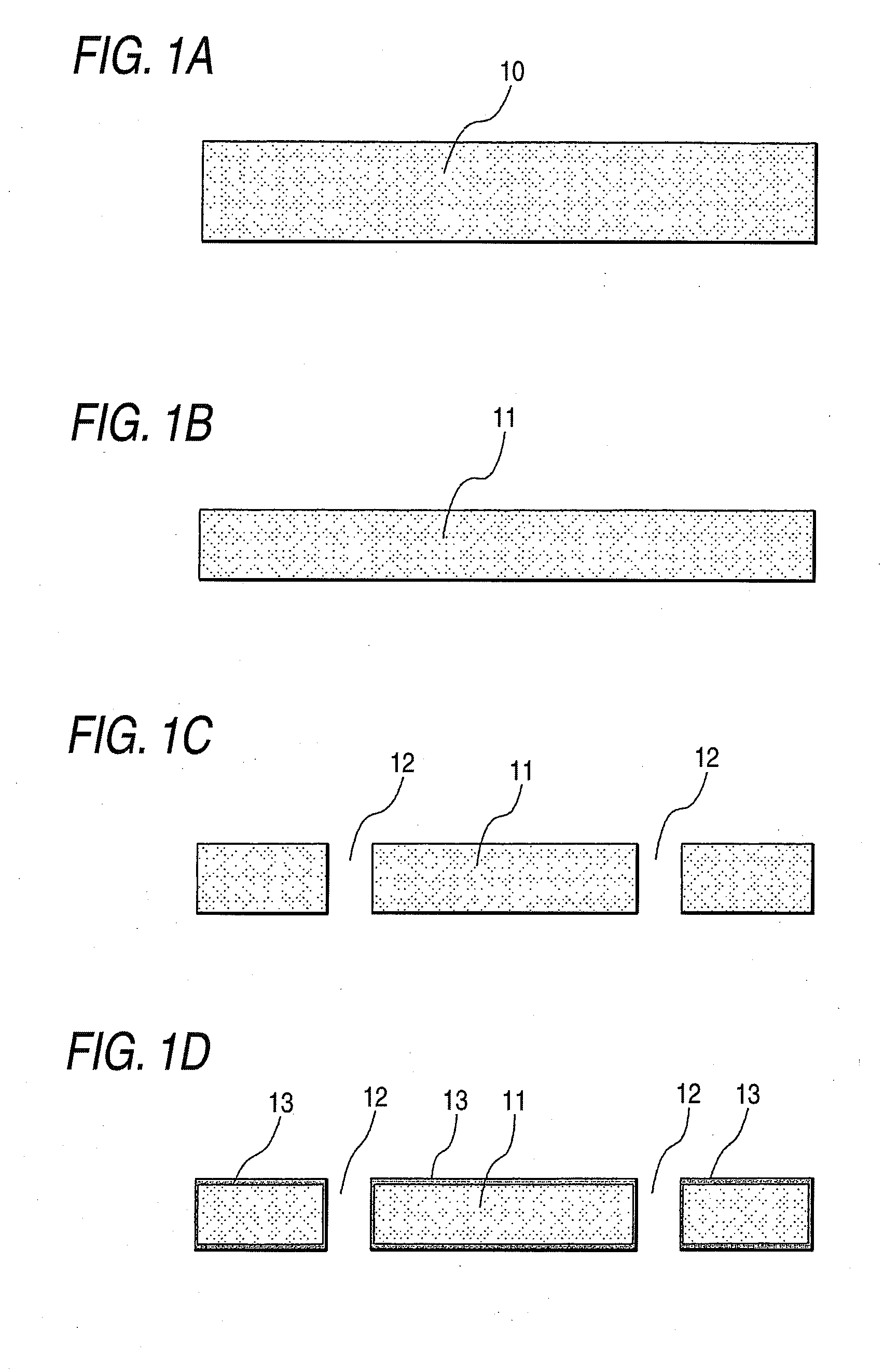
[0051]An embodiment of a silicon interposer according to the present invention will be described below on the basis of the drawings. FIGS. 1A to 1D and FIGS. 5A and 5B are sectional views showing the states at the periphery of through-hole electrodes in the respective production stages of the silicon interposer according to this embodiment.

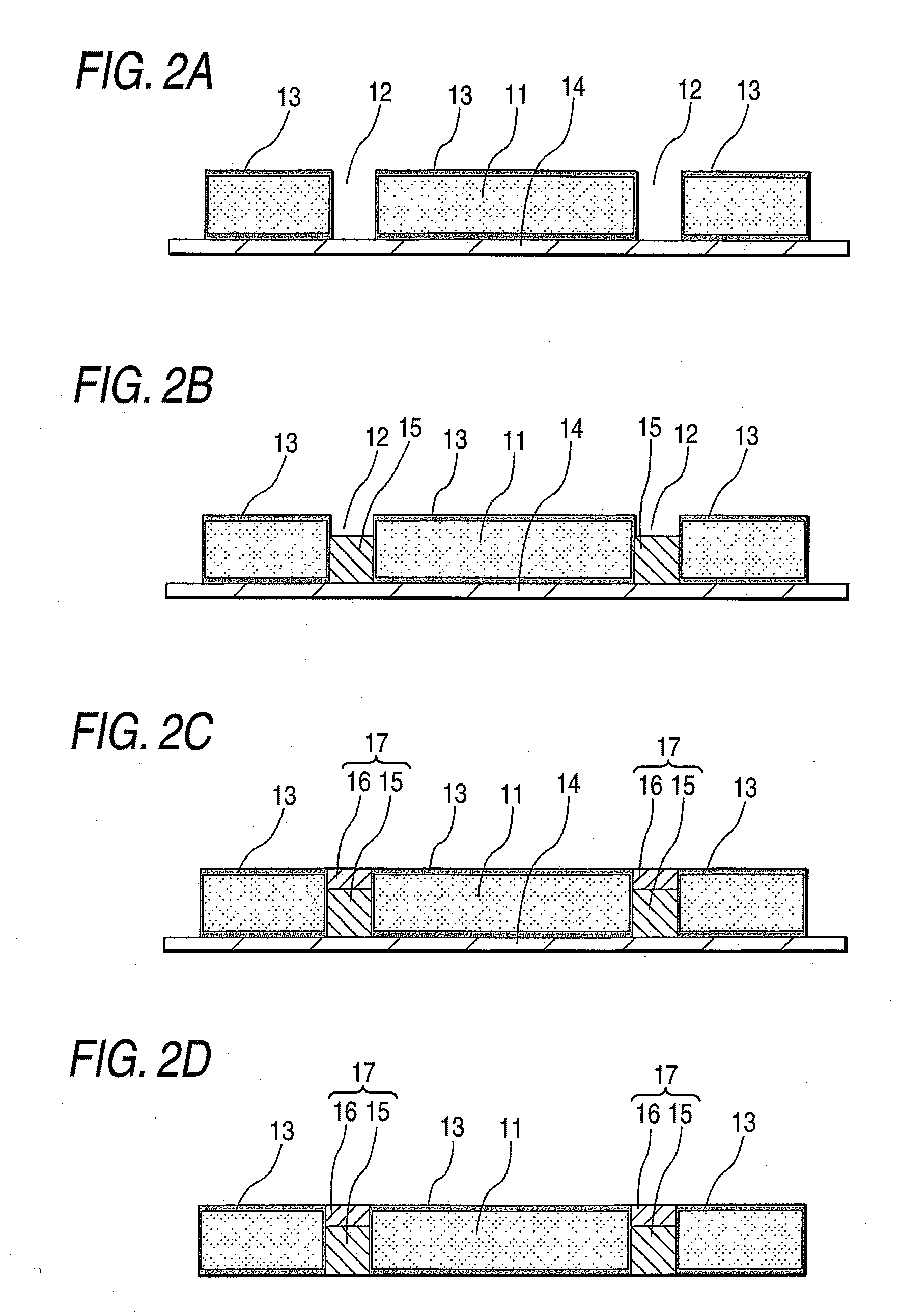
[0052]First, as shown in FIG. 1A, after a silicon wafer 10 is sliced, it is ground using a grinder or the like to a thickness of 300 μm. After the silicon wafer 10 is processed into a thin silicon wafer 11 shown in FIG. 1B, the surface of the thin silicon wafer 11 is covered with a mask having openings at regions where through holes 12 are formed, and etching is carried out, whereby the through holes 12 shown in FIG. 1C are formed. The through holes 12 according to this embodiment are formed so as to have a diameter of 60 μm. The through holes 12 are later filled with conductive materials so as to be formed into the through-hole electrodes 17 of a...

second embodiment

[0073]In the first embodiment, since the upper face side of the silicon interposer 30 in the figure is used as a face on which the semiconductor element 60 is mounted, the solder 16 serving as the buffer section for thermal stress is filled in a desired range on the copper 15 serving as the base section and filled in the through-hole electrode 17. However, the present invention is not limited to this configuration.

[0074]The present invention relates to a structure in which the buffer section for absorbing the thermal stress generated at the portion connected to the through-hole electrode 17 and having a thermal expansion coefficient significantly different from the thermal expansion coefficient of the base section (the copper 15) of the through-hole electrode 17 is provided between the base section (the copper 15) inside the through-hole electrode 17 and the connection sections of the through-hole electrode 17. Hence, even if the wiring board 40 is on the side on which the connectio...

third embodiment

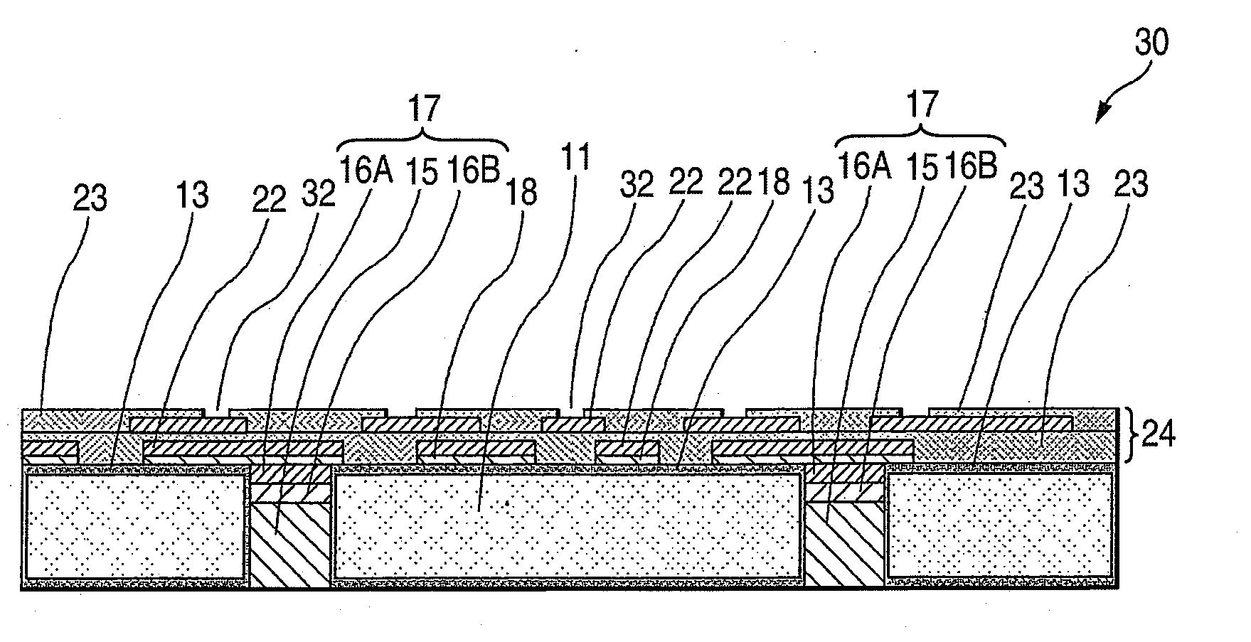
[0078]FIG. 10 is a sectional view showing the structure at the periphery of the through-hole electrodes of a silicon interposer according to a third embodiment. This embodiment is characterized in that the conductive materials filled in the buffer section of the through-hole electrode 17 are formed of conductive materials 16A and 16B that are different from each other and overlaid. In the case of this structure, it is preferable that the conductive materials 16A and 16B constituting the buffer section should be overlaid such that the elastic coefficient of the buffer section lowers gradually toward the exposed face of the through-hole electrode 17.

[0079]By virtue of the adoption of the configuration of the silicon interposer 30 according to this embodiment, the gradient (the gradient of elastic coefficient) of the deformation amount in the range of the buffer section to the base section inside the through-hole electrode 17 becomes moderate, and the reliability of the through-hole el...


PUM


Abstract

A silicon interposer 30 being held between a wiring board 40 and a semiconductor element 60 to electrically connect the wiring board 40 to the semiconductor element 60, wherein through-hole electrodes 17 for electrically connecting the wiring board 40 to the semiconductor element 60 are each formed of a base section and a buffer section, and the buffer section is formed of a conductive material having an elastic coefficient lower than that of the conductive material of the base section, and a semiconductor device package 50 and a semiconductor device 70 incorporating the silicon interposer 30.

Description

BACKGROUND OF THE INVENTION[0001]The present invention relates to a silicon interposer and a semiconductor device package and a semiconductor device incorporating the silicon interposer.[0002]In the case that a semiconductor device is produced, for example, by mounting semiconductor elements on a wiring board which is made of a glass epoxy material and on which a wiring pattern is formed, by carrying out soldering or the like, it is necessary to heat the wiring board and the semiconductor elements up to the solder melting temperature. At this time, since the thermal expansion coefficient of the wiring board made of a glass epoxy material is different from that of the semiconductor elements made of silicon, cracks may occur at the connection sections between the wiring board and the semiconductor elements and the semiconductor elements may be damaged when the wiring board and the semiconductor elements become cool after the completion of the soldering processing.[0003]For the purpose...

Claims


Application Information

Patent Timeline
Patent Type & Authority Applications(United States)
IPC IPC(8): H01L23/34H01L23/495
CPCH01L23/49816H01L23/49827H01L2224/16225H01L2224/32225H01L2224/73204H01L2924/15192H01L2924/15311H01L2924/157H01L2924/00H01L23/12
Inventor SUNOHARA, MASAHIRO
Owner SHINKO ELECTRIC IND CO LTD
Why Eureka
Try Eureka