Exposure method, exposure apparatus, and method for manufacturing device

a manufacturing device and exposure method technology, applied in the field of exposure techniques, can solve the problems of small improvement in the overall level and difficulty in accurately exposing only the imperfect shot regions of the wafer, and achieve the effect of efficient exposure and improved throughput of the exposure block

Inactive Publication Date: 2009-05-14
NIKON CORP
View PDF5 Cites 14 Cited by
  • Summary
  • Abstract
  • Description
  • Claims
  • Application Information

AI Technical Summary

Benefits of technology

[0012]In one embodiment of the present invention, the exposure of a first region (for example, region including perfect shot regions) of a first substrate on a first substrate movable holder is performed substantially parallel to the exposure of a second region (for example, portion including perfect shot regions) of a second substrate on a second substrate movable holder. Thus, patterns corresponding to the first and second regions can be efficiently exposed. Further, the detection of a mark (mark detection operation of second block) with an alignment system for exposing the first region of the second substrate is performed substantially parallel to the exposure of the second region of the substrate. This further improves throughput of the exposure block.

Problems solved by technology

Thus, it is difficult to accurately expose only the imperfect shot regions of a wafer.
Therefore, the level of improvement in throughout is small.

Method used


Image

  • Exposure method, exposure apparatus, and method for manufacturing device
  • Exposure method, exposure apparatus, and method for manufacturing device
  • Exposure method, exposure apparatus, and method for manufacturing device

Examples


Embodiment Construction

[0022]One example of a preferred embodiment according to the present invention will now be described with reference to the drawings.

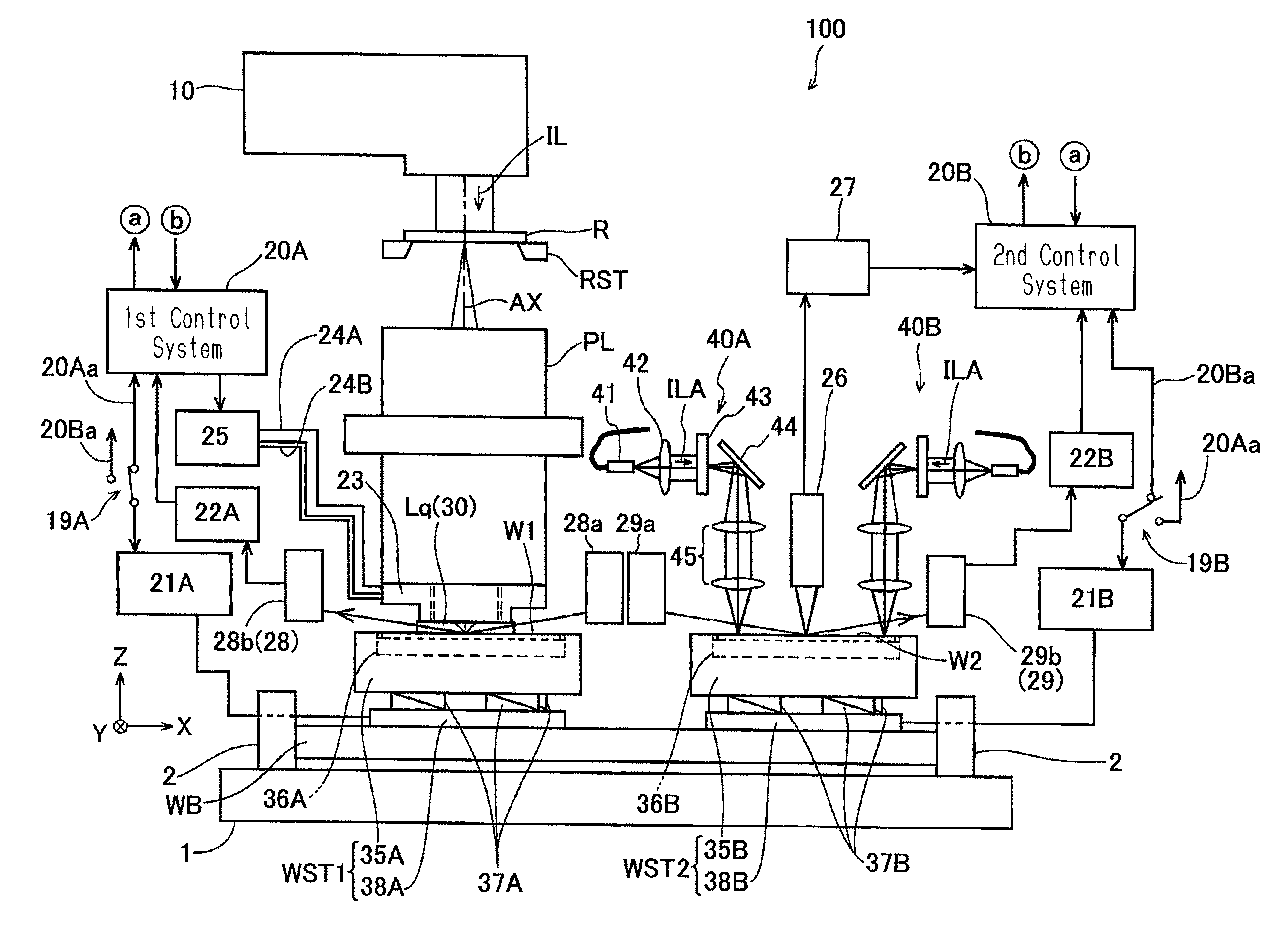
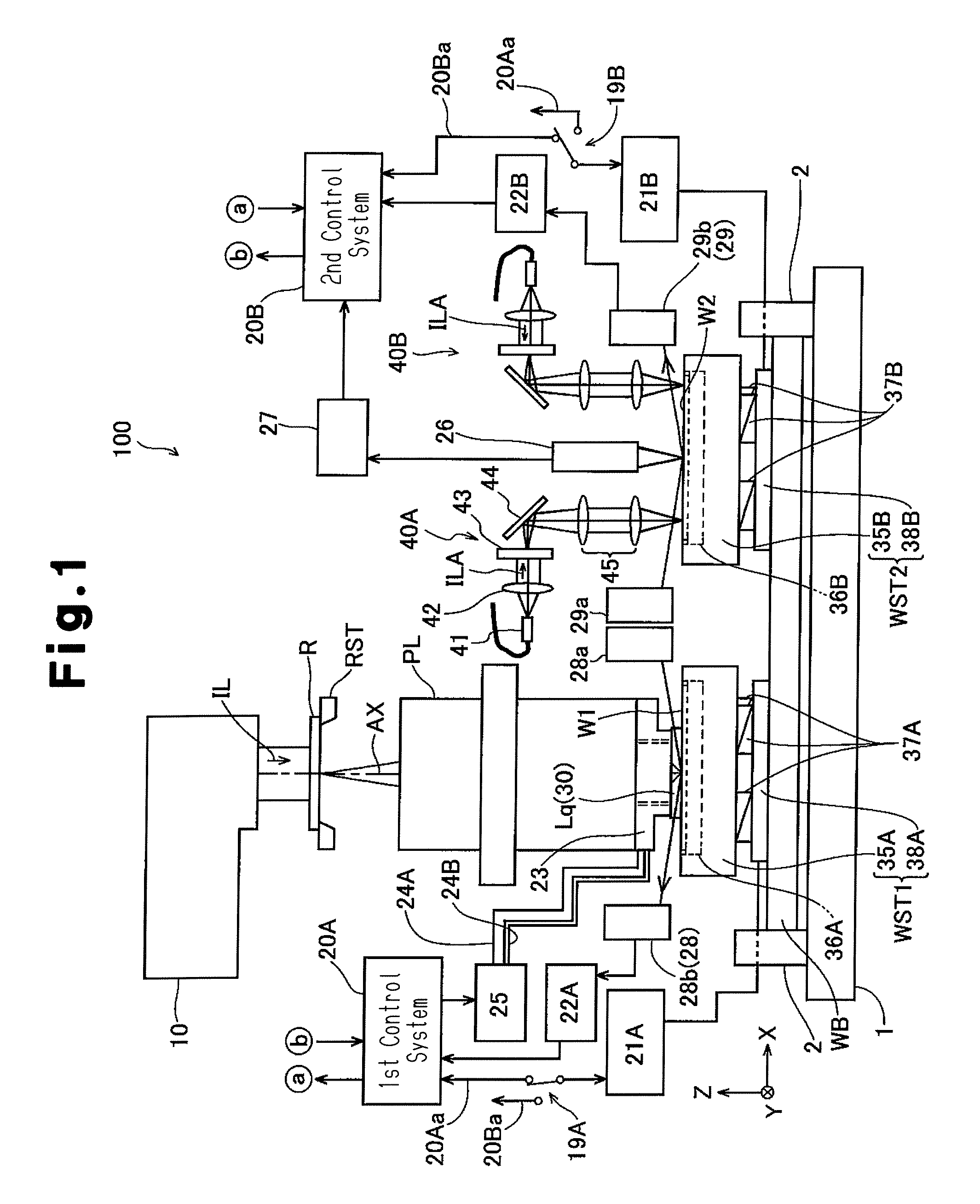
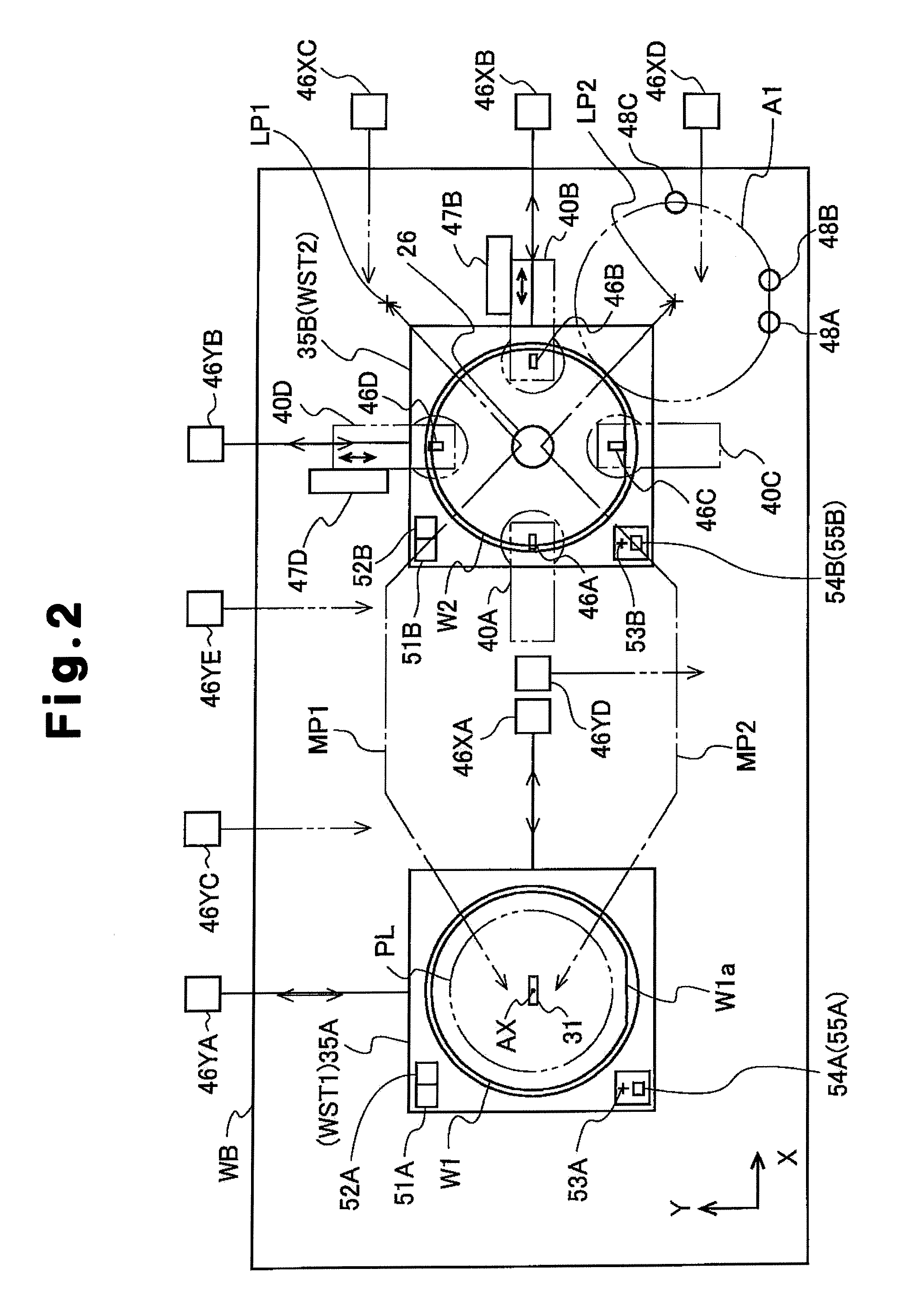
[0023]FIG. 1 is a schematic diagram showing an exposure apparatus 100 of the present embodiment. The exposure apparatus 100 is a projection exposure apparatus of a scanning exposure type that includes a scanning stepper (scanner) and performs exposure through liquid immersion.

[0024]In FIG. 1, the exposure apparatus 100 includes an illumination system 10, a reticle stage RST, a projection optical system PL, a first wafer stage WST1, and a first control system 20A. The illumination system 10, which includes a light source and an illumination optical system, illuminates a reticle R (mask) with exposure light IL (illumination light used for exposure) serving as an exposure beam. The reticle stage RST holds and moves the reticle R. The projection optical system PL exposes a region on a wafer (in FIG. 1, wafer W1), which serves as a substrate, including a dev...


PUM

PropertyMeasurementUnit
oscillation wavelengthaaaaaaaaaa
wavelengthaaaaaaaaaa
diameteraaaaaaaaaa

Abstract

An exposure apparatus for efficiently exposing patterns onto corresponding regions of a substrate. The apparatus includes a first wafer stage, a second wafer stage, an alignment sensor which detects marks of wafers on the wafer stages, a projection optical system which irradiates a first region of a wafer with first exposure light, and an imperfect shot region exposure system which irradiates a second region of a wafer that differs from the first region with second exposure light. The imperfect shot region exposure system irradiates the second region of a wafer held on the second wafer stage with the second exposure light.

Description

CROSS-REFERENCE TO RELATED APPLICATIONS[0001]This application claims the benefit of U.S. Provisional Application No. 60 / 996,379, filed on Nov. 14, 2007.BACKGROUND[0002]The present disclosure relates to an exposure technique for exposing a plurality of different regions on a substrate that is, for example, applicable when exposing onto an imperfect shot region of a substrate a pattern that is to be exposed onto a perfect shot region of the substrate. The present disclosure further relates to a technique for manufacturing a device using the exposure technique.[0003]In a lithography process for manufacturing various types of devices (electronic devices and micro-devices), for example, semiconductor devices, liquid crystal display devices, and the like, an exposure apparatus such as a batch exposure type projection exposure apparatus like a stepper and the like or a scanning exposure type projection exposure apparatus (scanning type exposure apparatus) like a scanning stepper or the lik...

Claims


Application Information

Patent Timeline
Patent Type & Authority Applications(United States)
IPC IPC(8): G03F7/20G03B27/32G03B27/42
CPCG03F7/70525G03F9/7096G03F7/70733
Inventor NAGAYAMA, TADASHI
Owner NIKON CORP
Why Eureka
Try Eureka