Low temperature deposition of phase change memory materials

a memory material and low temperature technology, applied in the field of low temperature deposition of phase change memory materials, can solve the problems of reducing the efficiency of the product pcm devi

Inactive Publication Date: 2009-05-14
ENTEGRIS INC
View PDF54 Cites 77 Cited by
  • Summary
  • Abstract
  • Description
  • Claims
  • Application Information

AI Technical Summary

Benefits of technology

[0015]Additional aspects of the invention relate to PCM films formed in accordance with the present invention; corresponding devices; tellurium complexes, germanium complexes, germanium tellurides, and processes utilizing same for forming GST films; compositions including combinations of precursors for forming PCM films; and packaged precursors adapted for coupling to a deposition tool comprising such compositions, as hereinafter more fully described.

Problems solved by technology

A major deficiency in the current art is the requirement of high deposition temperatures needed for conventionally employed alkyl (e.g., Me3Sb, Me2Te) or halide sources.
These temperatures are typically well in excess of 300° C., and may for example be on the order of 500° C. Such high temperatures substantially exceed the thermal budget for device integration and can result in the evaporation of the chalcogenide, rendering the product PCM device deficient or even useless for its intended purpose.

Method used


Image

  • Low temperature deposition of phase change memory materials
  • Low temperature deposition of phase change memory materials
  • Low temperature deposition of phase change memory materials

Examples


Embodiment Construction

[0019]The present invention relates to deposition of phase change memory materials to form PCM devices.

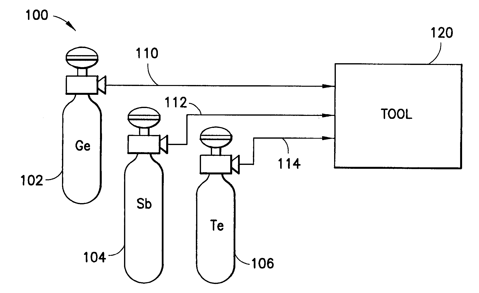
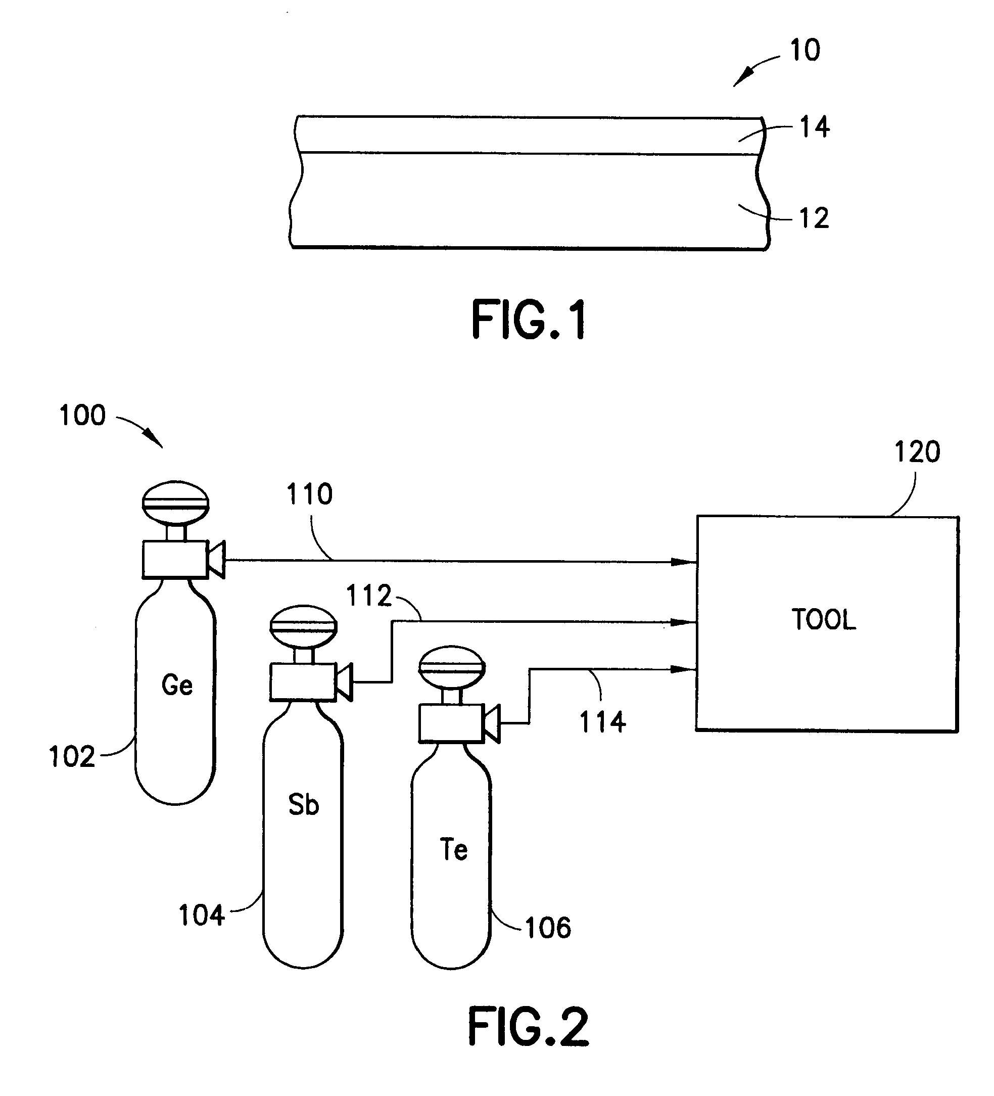
[0020]More specifically, the invention in one aspect relates to chalcogenide alloys, and to their low temperature deposition e.g., by chemical vapor deposition (CVD) or atomic layer deposition (ALD), to form PCM devices. CVD and ALD methods are employed in the practice of the present invention to achieve scalability to large area wafers and for composition control. Preferred chalconide alloys include alloys including two or more of germanium, antimony and tellurium.

[0021]As used herein, the term “low temperature” means a temperature below 350° C. The temperature at which the PCM material is deposited is preferably less than 300° C., more preferably less than 250° C. and most preferably less than 225° C.

[0022]In one aspect, the invention relates to a method of forming a phase change memory material on a substrate, comprising contacting the substrate with precursors for a phase chang...


PUM

PropertyMeasurementUnit
temperatureaaaaaaaaaa
temperaturesaaaaaaaaaa

Abstract

A system and method for forming a phase change memory material on a substrate, in which the substrate is contacted with precursors for a phase change memory chalcogenide alloy under conditions producing deposition of the chalcogenide alloy on the substrate, at temperature below 350° C. with the contacting being carried out via chemical vapor deposition or atomic layer deposition. Various tellurium, germanium and germanium-tellurium precursors are described, which are useful for forming GST phase change memory films on substrates.

Description

BACKGROUND OF THE INVENTION[0001]1. Field of the Invention[0002]The present invention relates to low temperature deposition of phase change memory materials, by deposition techniques such as chemical vapor deposition and atomic layer deposition, to form microelectronic device structures.[0003]2. Description of the Related Art[0004]Phase Change Memory (PCM) refers to a novel memory technology based on chalcogenide materials that undergo a phase change via a heater and are read out as “0” or “1” based on their electrical resistivity, which changes in correspondence to whether the phase change material in the cell is in the crystalline or amorphous phase.[0005]The chalcogenide materials used in PCM comprise a large number of binary, ternary, and quaternary alloys of a number of metals and metalloids. Examples include GeSbTe, GeSbInTe, and many others. As contained herein, the identification of compounds such as GeSbTe and GeSbInTe without appertaining stoichiometric coefficients or val...

Claims


Application Information

Patent Timeline
Patent Type & Authority Applications(United States)
IPC IPC(8): H01L51/30H01L21/06C07D401/02C07F7/30C07F7/08
CPCC07F7/30H01L51/0002C23C16/45553C23C16/305H10N70/231H10N70/882H10K71/10
Inventor ROEDER, JEFFREY F.BAUM, THOMAS H.HENDRIX, BRYAN C.STAUF, GREGORY T.XU, CHONGYINGHUNKS, WILLIAMCHEN, TIANNIUSTENDER, MATTHIAS
Owner ENTEGRIS INC
Why Eureka
Try Eureka