High frequency electronic component

Inactive Publication Date: 2009-05-21
TDK CORPARATION
View PDF11 Cites 19 Cited by
  • Summary
  • Abstract
  • Description
  • Claims
  • Application Information

AI Technical Summary

Benefits of technology

[0023]It is an object of the present invention to provide a high frequency electronic component for use in a signal processing circuit that processes a plurality of high frequency signals, i.e., a plurality of transmission signals or

Problems solved by technology

The power amplifier is more expensive than other electronic components constituting the transmission circuit.
In a multi-mode-capable cellular phone having communication functions for both the GSM system and the UMTS, however, a single power amplifier is not shared between the GSM system and the UMTS.
The transmission circuit thus requires a plurality of power amplifiers, each of which is relatively expensive as previously mentioned, and this impedes reductions in size and cost of the cellular phone.
However, such a configuration deals with only a transmission signal in the form of an unbalanced signal, and therefore cannot use a balanced input power amplifier that has been proposed in many publications as described above.
In a cellular phone capable of operating under the GSM system and the UMTS, in many cases, the GSM transmission signal is generated in the form of a balanced signal and the UMTS transmission signal is generated in the form of an unbalanced signal by the integrated circuit.
In the case where a transmission signal in the form of a balanced signal and a transmission signal in the form of an unbalanced signal both exist as above, the common use of a single power amplifier for both the transmission signal in the form of a balanced signal and the transmission signal in the form of an unbalanced signal is not possible.
However, a switch for switching between balanced signals is more expensive than a switch for switching between unbalanced signals.
Consequently, while the configuration in which a switch for switching between balanced signals is provided before the balanced input power amplifier allows a cost reduction by reducing the number of the power amplifiers, it causes a cost increase on the other hand, because of the use of the switch for switching between balanced signals.
The low-noise amplifier is more expensive than other electronic components constituting the reception circuit.
This is detrimental to miniaturization of cellular phones.
In addit

Method used


Image

  • High frequency electronic component
  • High frequency electronic component
  • High frequency electronic component

Examples


first embodiment

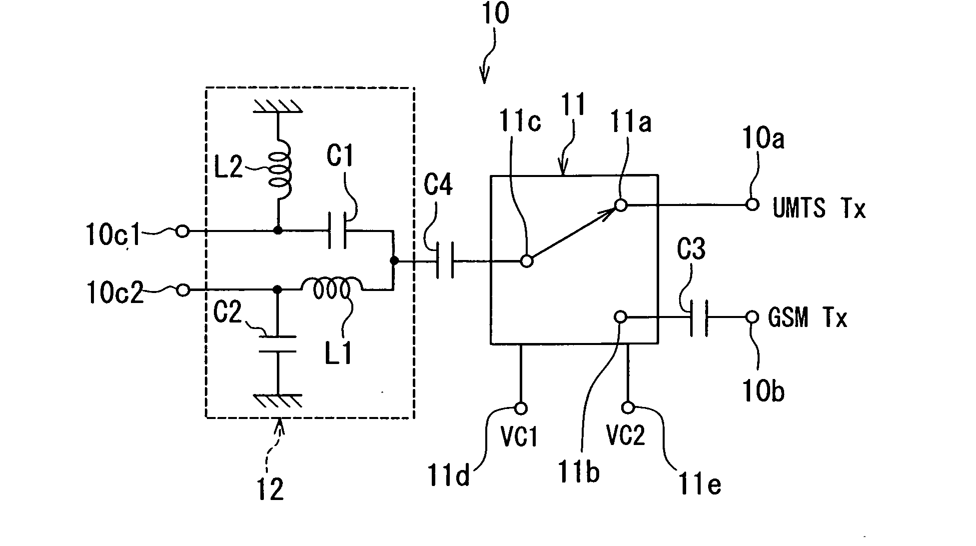
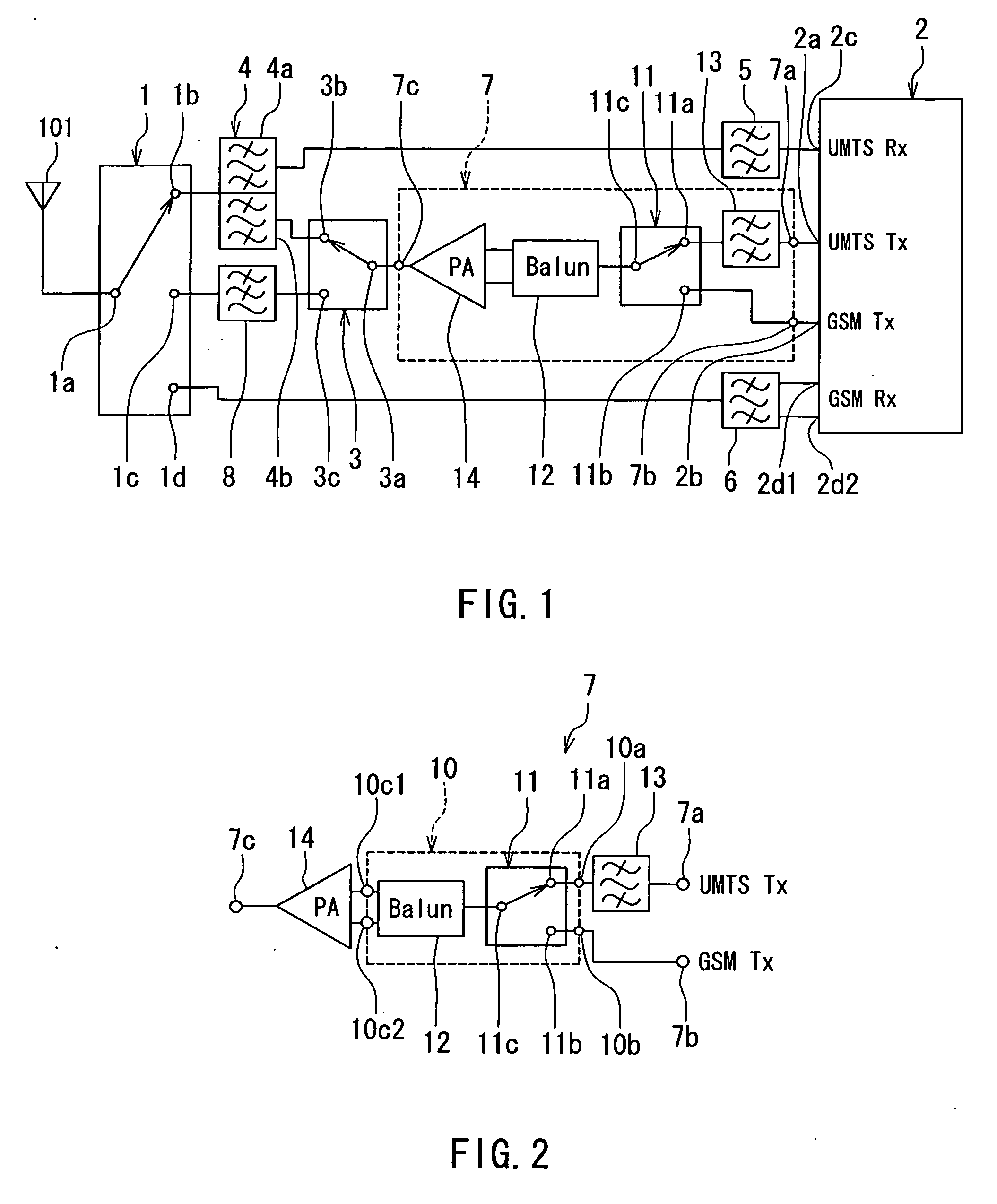
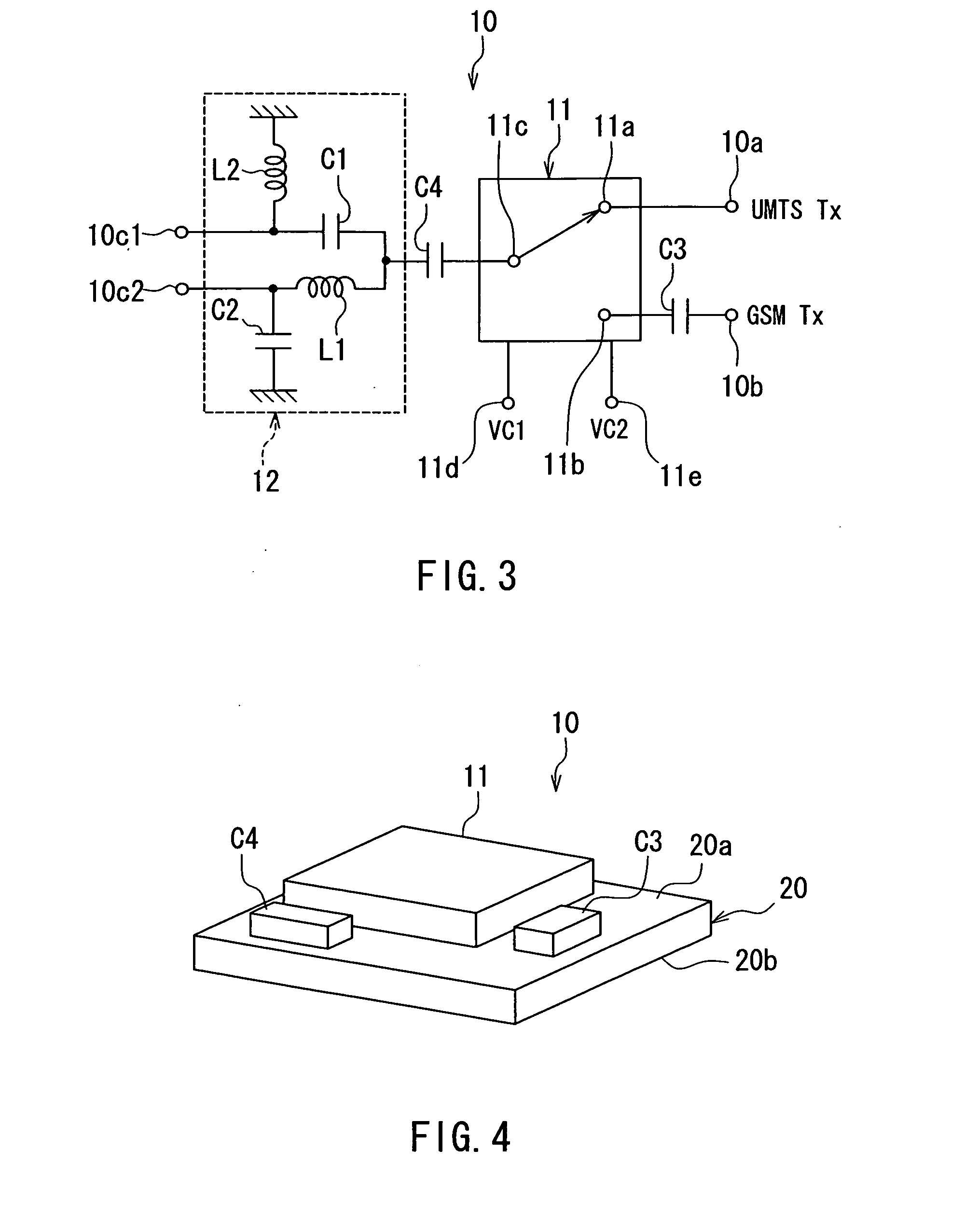
[0080]Preferred embodiments of the present invention will now be described in detail with reference to the drawings. Reference is first made to FIG. 1 to describe an example of a high frequency circuit of a cellular phone including a high frequency electronic component of a first embodiment of the invention. FIG. 1 is a block diagram illustrating the circuit configuration of this example of high frequency circuit. This high frequency circuit processes a signal of the GSM system, which is based on the TDMA system, and a signal of the UMTS, which is based on the WCDMA system.

[0081]Table 1 shows the types of GSM signals, and Table 2 shows the types of UMTS signals. In Tables 1 and 2 the “Uplink” columns show the frequency bands of transmission signals, and the “Downlink” columns show the frequency bands of reception signals.

TABLE 1SystemFrequency bandUplink (MHz)Downlink (MHz)GSM850850 MHz band824-849869-894(AGSM)GSM900 (EGSM)900 MHz band880-915925-960GSM1800 (DCS)1800 MHz band 1710-17...

second embodiment

[0131]A high frequency electronic component of a second embodiment of the invention will now be described with reference to FIG. 14. FIG. 14 shows a transmission circuit 7 including the high frequency electronic component 10 of the second embodiment. In the second embodiment, the IC 2 generates and outputs a transmission signal GSM Tx in the form of a balanced signal, not in the form of an unbalanced signal. The transmission circuit 7 of the second embodiment includes a balun 15, in addition to the components of the transmission circuit 7 of the first embodiment. The balun 15 has two balanced inputs and an unbalanced output. The two balanced inputs of the balun 15 are connected to terminals of the IC2 that output the transmission signal GSM Tx in the form of a balanced signal. The unbalanced output of the balun 15 is connected to the input terminal 10b of the high frequency electronic component 10. The balun 15 converts the transmission signal GSM Tx in the form of a balanced signal...

third embodiment

[0141]A high frequency electronic component of a third embodiment of the invention will now be described with reference to FIG. 18. FIG. 18 shows a transmission circuit 7 including the high frequency electronic component 40 of the third embodiment. The high frequency electronic component 40 of the third embodiment is for use in the transmission circuit 7 that processes two UMTS transmission signals UMTS Tx1 and UMTS Tx2 and a GSM transmission signal GSM Tx. In the third embodiment, in the case where the transmission signal GSM Tx is a transmission signal of at least one of GSM850 (AGSM) and GSM900 (EGSM), the transmission signals UMTS Tx1 and UMTS Tx2 are transmission signals of two different bands among the bands V, VI and VIII whose frequency bands are close to those of GSM850 (AGSM) and GSM900 (ESGM). In the case where the transmission signal GSM Tx is a transmission signal of at least one of GSM1800 (DCS) and GSM1900 (PCS), the transmission signals UMTS Tx1 and UMTS Tx2 are tran...


PUM


Abstract

A high frequency electronic component includes a switch and a balun. The switch performs switching between a first transmission signal in the form of an unbalanced signal received at a first input port and a second transmission signal in the form of an unbalanced signal received at a second input port, and outputs one of the first and second transmission signals from an output port. The balun converts the transmission signal in the form of an unbalanced signal outputted form the output port of the switch to a transmission signal in the form of a balanced signal, and outputs this signal to a balanced input power amplifier.

Description

BACKGROUND OF THE INVENTION[0001]1. Field of the Invention[0002]The present invention relates to a high frequency electronic component for use in a signal processing circuit that processes a plurality of high frequency signals, and more specifically, to a high frequency electronic component for use in a transmission circuit that processes a plurality of transmission signals or a reception circuit that processes a plurality of reception signals.[0003]2. Description of the Related Art[0004]Recently, cellular phones capable of operating in a plurality of frequency bands (multi-bands) have been put to practical use. The third-generation cellular phones having a high-rate data communication function have also been widely used. Accordingly, multi-mode and multi-band capability is demanded of cellular phones.[0005]For example, cellular phones conforming to the time division multiple access (TDMA) system and having multi-band capability are in practical use. Cellular phones conforming to th...

Claims


Application Information

Patent Timeline
IPC IPC(8): H01P1/10
CPCH03H7/465H04B1/0067H04B1/006
Inventor GOI, TOMOYUKINAGAI, KENTAHARADA, NOBUMIMIURA, MITSURUYOSHIDA, SHUICHI
Owner TDK CORPARATION
Why Eureka
Try Eureka