Multiplier device with suppression of higher-order distortion

US20090138744A1Inactive Publication Date: 2009-05-28KASPERKOVITZ WOLFDIETRICH GEORG
2 Cites 5 Cited by

Patent Information

Authority / Receiving Office
US Ā· United States
Current Assignee / Owner
Publication Date
2009-05-28
Estimated Expiration
Not applicable Ā· inactive patent

Smart Images

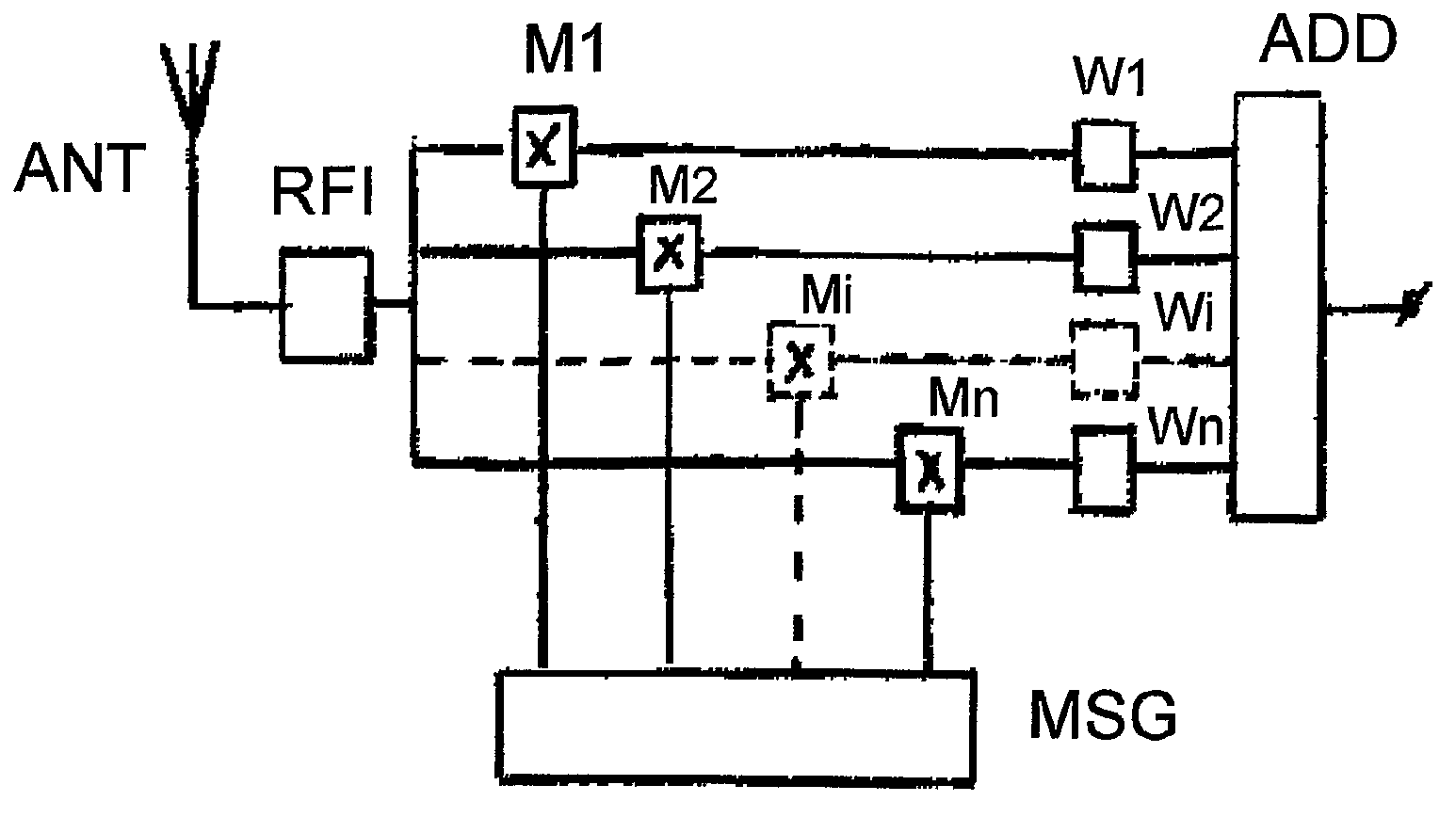
  • Figure 1
    Figure 1
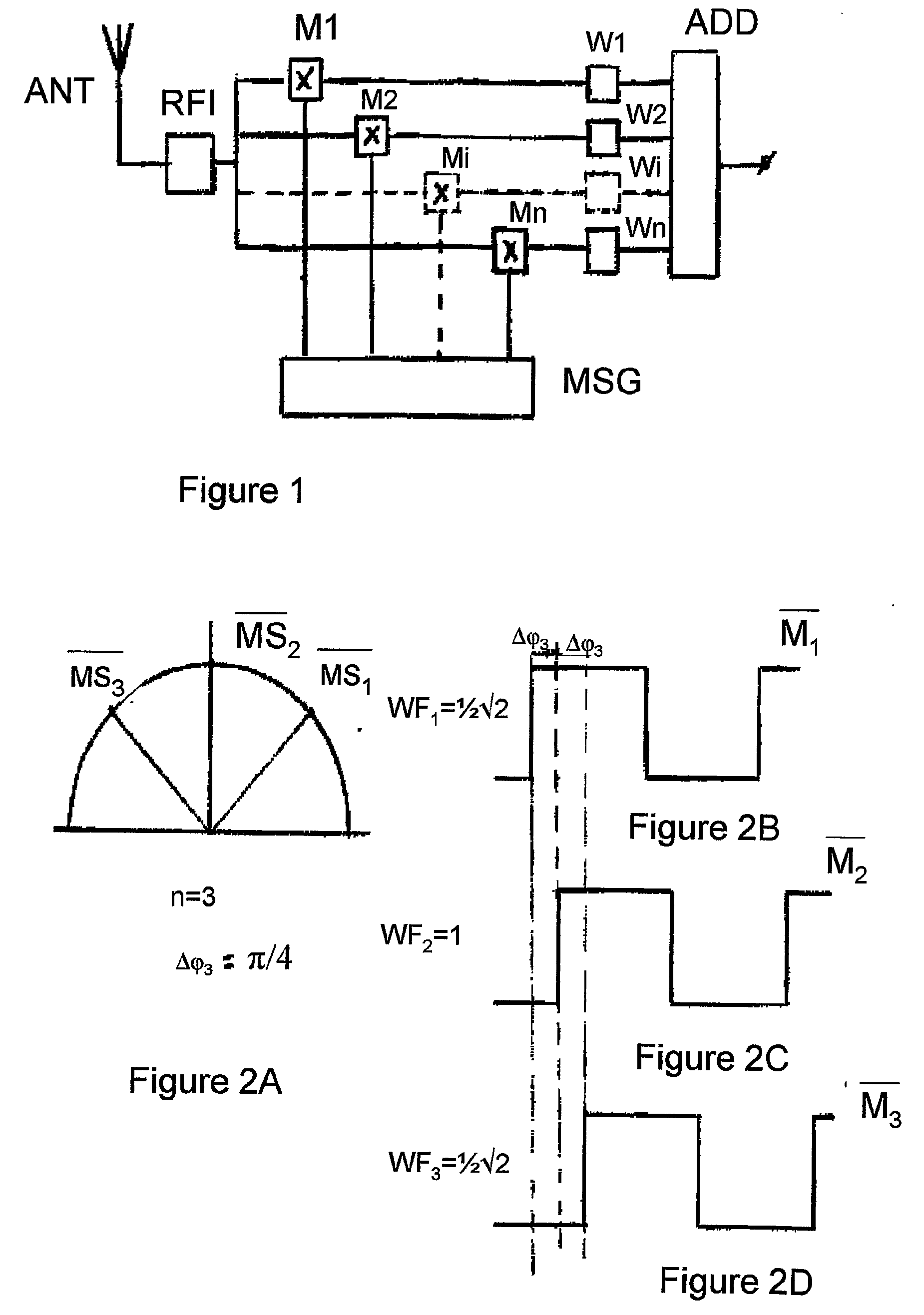
  • Figure 2
    Figure 2
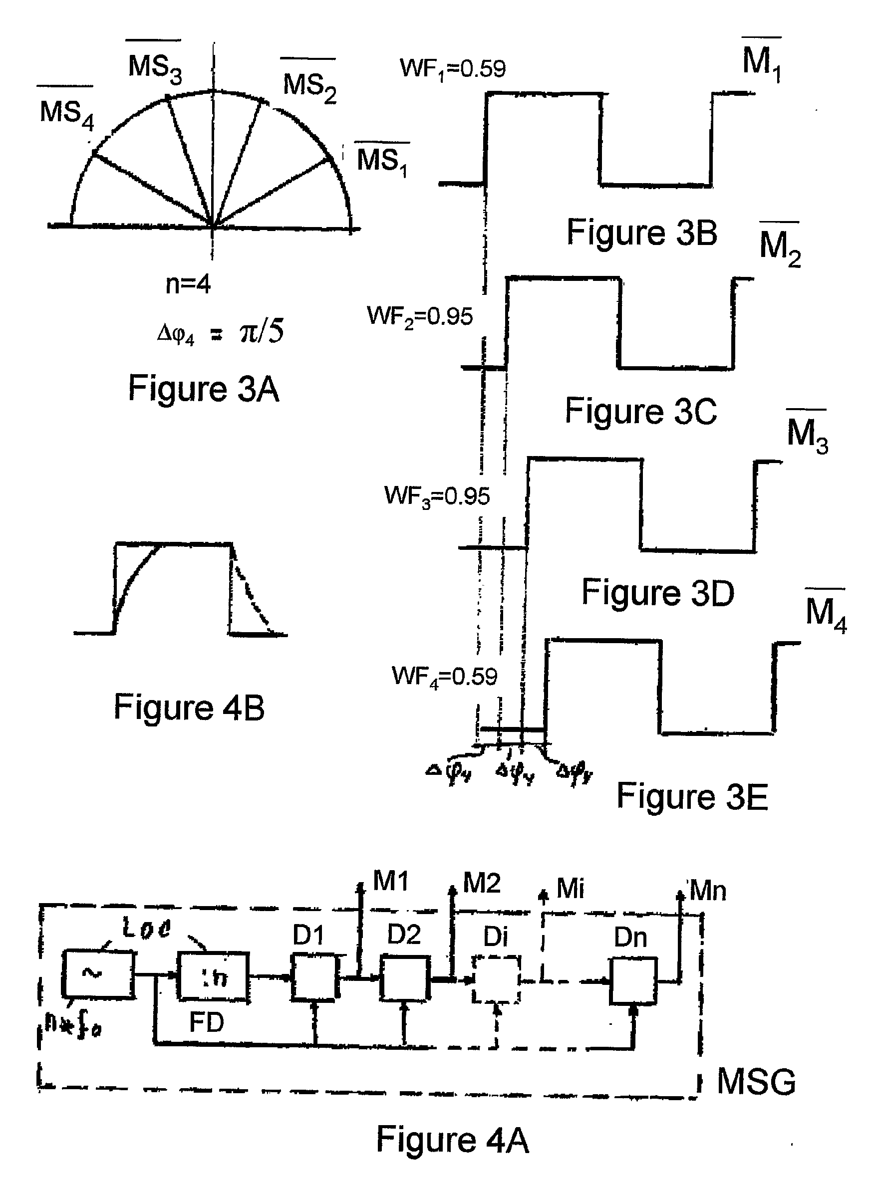
  • Figure 3
    Figure 3
Patent Text Reader

Abstract

A multiplier device is configured to include first to nth multipliers M1 to Mn for multiplying a carrier modulated information signal with first to nth mutually phase shifted and identical, substantially square wave mixing signals MS1 to MSn with 50% duty cycle. In order to eliminate fifth or higher order interferences from the output of the multiplier device according to the invention, n is greater than 2, outputs of the multipliers M1 to Mn are respectively coupled through weighting circuits W1 to Wn with respective fixed weighting factors WF1 to WFn to an adder circuit, the mixing signals MS1 to MSn having respective phase angles φi corresponding to φi=i*Δφ, the weighting factors WFi corresponding to the sine value of the respective phase angles φi=i*Δφ with Δφ being the mutual phase difference between each two phase consecutive mixing signals corresponding to Ļ€ / (n+1) and i varying from 1 to n.
Need to check novelty before this filing date? Find Prior Art

Description

[0001] This application is a continuation of U.S. patent application Ser. No. 10 / 581,659, filed 31 May 2006, and claims the benefit of PCT / EP2004 / 013742, filed 1 Dec. 2004 and EP 03078812, filed 5 Dec. 2003.BACKGROUND AND SUMMARY OF THE INVENTION

[0002] The invention relates to a multiplier device comprising first to nth multipliers M1 to Mn for multiplying a carrier modulated information signal with first to nth mutually phase shifted and identical, substantially square wave mixing signals MS1 to MSn with 50% duty cycle. Such multiplier devices are frequently used in receivers for converting an RF antenna input signal with an RF carrier frequency fRF into an intermediate frequency (IF) signal with an IF carrier frequency fIF and / or for demodulating an (IF) carrier modulated information signal with carrier frequency fc into baseband, or as used in stereo decoder circuits for decoding and / or demultiplexing a stereo multiplex signal into left and right baseband stereo signals.

[0003] A ste...

Examples

Embodiment Construction

[0024]FIG. 1 shows an embodiment of a multiplier device (M1-Mn, W1-Wn, ADD) according to the invention used in a receiver front end. The receiver front end comprises an RF antenna ANT being coupled to an RF input unit RFI supplying an RF antenna input signal with an RF carrier frequency fRF in common to first to nth multipliers M1 to Mn, n being 3 or more. The RF antenna input signal is being demodulated therein into an intermediate frequency (IF) signal with an IF carrier frequency fIF. The first to nth multipliers M1 to Mn receive from a mixing signal generator MSG respectively first to nth mutually phase shifted and identical, substantially square wave mixing signals MS1 to MSn with 50% duty cycle. Outputs of the first to nth multipliers M1 to Mn are respectively coupled through weighting circuits W1 to Wn with respective fixed weighting factors WF1 to WFn to an adder circuit ADD. The adder circuit ADD provides at its output the IF signal without harmonic interferences up to the ...