Light output enhanced gallium nitride based thin light emitting diode

a technology of light emitting diodes and gallium nitride, which is applied in the direction of semiconductor devices, lighting and heating apparatus, refractors, etc., can solve the problems of low internal efficiency, low dislocation density, and decreased light extraction efficiency (lee) through the gan crystal, so as to reduce re-absorption of light, increase internal quantum efficiency, and reduce the effect of re-absorption

Inactive Publication Date: 2009-06-04
RGT UNIV OF CALIFORNIA
View PDF12 Cites 50 Cited by
  • Summary
  • Abstract
  • Description
  • Claims
  • Application Information

AI Technical Summary

Benefits of technology

[0019]The present invention further discloses a method for increasing internal quantum efficiency (IQE) of a III-nitride light emitting device by reducing re-absorption of light by the device, comprising: providing an active region for emitting the light; and providing one or more thicknesses of III-nitride between the active region and one or more light extraction or reflection surfaces of the light emitting device, wherein the thicknesses are such that an intensity of the light at the extraction surfaces is attenuated by no more than 5% as compared to the intensity of the light at the active region, wherein the attenuation is due to absorption of the light by the III-nitride.
[0020]Finally, the present invention discloses a method for emitting light from a light emitting device with increased internal quantum efficiency, comprising: emitting light from an active region of the device, wherein one or more thicknesses of III-nitride, between the active region and one or more light extraction or reflection surfaces of the light emitting device, are such that an intensity of the light at the extraction surfaces is attenuated by no more than 5% as compared to the intensity of the light at the active region, wherein the attenuation is due to absorption of the light by the III-nitride.

Problems solved by technology

However, light extraction efficiency (LEE) is decreased through the GaN crystal due to free carrier absorption.
The dislocation density is still high and internal efficiency is low.

Method used


Image

  • Light output enhanced gallium nitride based thin light emitting diode
  • Light output enhanced gallium nitride based thin light emitting diode
  • Light output enhanced gallium nitride based thin light emitting diode

Examples


Embodiment Construction

[0028]In the following description of the preferred embodiment, reference is made to the accompanying drawings which form a part hereof, and in which is shown by way of illustration a specific embodiment in which the invention may be practiced. It is to be understood that other embodiments may be utilized and structural changes may be made without departing from the scope of the present invention.

[0029]Technical Description

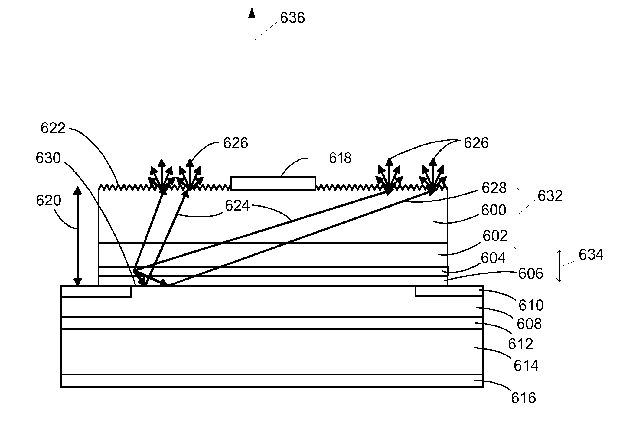
[0030]To keep both IQE and LEE high, the present invention uses a GaN FSS which is made thinner. FIGS. 4a-4e illustrate a process for fabricating a device according to the preferred embodiment of the present invention.

[0031]FIG. 4a represents the step of MOCVD growth, comprising selecting a GaN substrate 400 having a desired crystallographic plane (non-polar, semi-polar or polar planes, for example) and growing a GaN LED structure on the substrate 400. The GaN substrate 400 may be a temporary substrate such as a GaN FSS. Basic growth layers comprise at least n-GaN...


PUM

PropertyMeasurementUnit
reflectivityaaaaaaaaaa
distanceaaaaaaaaaa
thicknessaaaaaaaaaa

Abstract

A gallium nitride (GaN) based light emitting device, wherein the device comprises a first surface and a second surface, and the first surface and second surface are separated by a thickness of less than 100 micrometers, and preferably less than 20 micrometers. The first surface may be roughened or textured. A silver or silver alloy may be deposited on the second surface. The second surface of the device may be bonded to a permanent substrate.

Description

CROSS REFERENCE TO RELATED APPLICATIONS[0001]This application claims the benefit under 35 U.S.C. Section 119(e) of co-pending and commonly-assigned U.S. Provisional Patent Application Ser. No. 60 / 991,625, filed on Nov. 30, 2007, by Junichi Sonoda, Shuji Nakamura, Kenji Iso, Steven P. DenBaars, and Makoto Saito, entitled “LIGHT OUTPUT ENHANCED GALLIUM NITRIDE BASED THIN LIGHT EMITTING DIODE,” attorneys' docket number 30794.250-US-P1 (2008-197-1), which application is incorporated by reference herein.[0002]This application is related to the following co-pending and commonly-assigned U.S. patent applications:[0003]U.S. Utility application Ser. No. 11 / 510,240, filed on Aug. 25, 2006, by P. Morgan Pattison, Rajat Sharma, Steven P. DenBaars, and Shuji Nakamura entitled “SEMICONDUCTOR MICRO-CAVITY LIGHT EMITTING DIODE,” attorney's docket number 30794.146-US-U1 (2006-017-2), which application claims the benefit under U.S.C. Section 119(e) of U.S. Provisional Application Ser. No. 60 / 711,940,...

Claims


Application Information

Patent Timeline
Patent Type & Authority Applications(United States)
IPC IPC(8): H01L33/00H01L21/20H01L33/02H01L33/22H01L33/40
CPCH01L33/0079H01L33/02H01L33/44H01L33/405H01L33/22H01L33/0093
Inventor SONODA, JUNICHINAKAMURA, SHUJIISO, KENJIDENBAARS, STEVEN P.SAITO, MAKOTO
Owner RGT UNIV OF CALIFORNIA
Why Eureka
Try Eureka