Polishing apparatus and polishing method

Active Publication Date: 2009-06-04
EBARA CORP
View PDF7 Cites 55 Cited by
  • Summary
  • Abstract
  • Description
  • Claims
  • Application Information

AI Technical Summary

Benefits of technology

[0044]According to the present invention, the plural polishing heads holding the polishing tapes with different roughness can be used to polish a substrate. The polishing head, that has terminated its polishing operation, is tilted to another polishing angle via a tilting motion, and another polishing head can further polish the sam

Problems solved by technology

As a result, unwanted films and a roughened surface are formed on a periphery of the wafer which is not used for products.
Under such circumstances, the unwanted films could come off the periphery onto devices formed on the wafer during several processes, resulting in a lowered yield.
However, in these conventional apparatuses, a long polishing time is required as a whole, because finish polishing is performed afte

Method used


Image

  • Polishing apparatus and polishing method
  • Polishing apparatus and polishing method
  • Polishing apparatus and polishing method

Examples


first embodiment

[0118]The polishing apparatus as described above is suitable for use in polishing a bevel portion of the wafer W. FIG. 6 is an enlarged cross-sectional view showing the periphery of the wafer W. An area where devices are formed is a flat portion D located inwardly of an edge surface G by several millimeters. As shown in FIG. 6, in this specification, a flat portion outwardly of the device formation area is defined as a near edge portion E, and an inclined portion including an upper slope F, the edge surface G, and a lower slope F is defined as a bevel portion B.

[0119]FIG. 7A is a view showing a state in which the polishing head assembly 1A is moved forward by the linear actuator 67 so as to press the polishing tape 23 against the bevel portion of the wafer W. The rotary holding mechanism 3 rotates the wafer W thereon so as to provide relative movement between the polishing tape 23 and the bevel portion of the wafer W, thereby polishing the bevel portion. FIG. 7B is a view showing a...

second embodiment

[0135]Next, the present invention will be described.

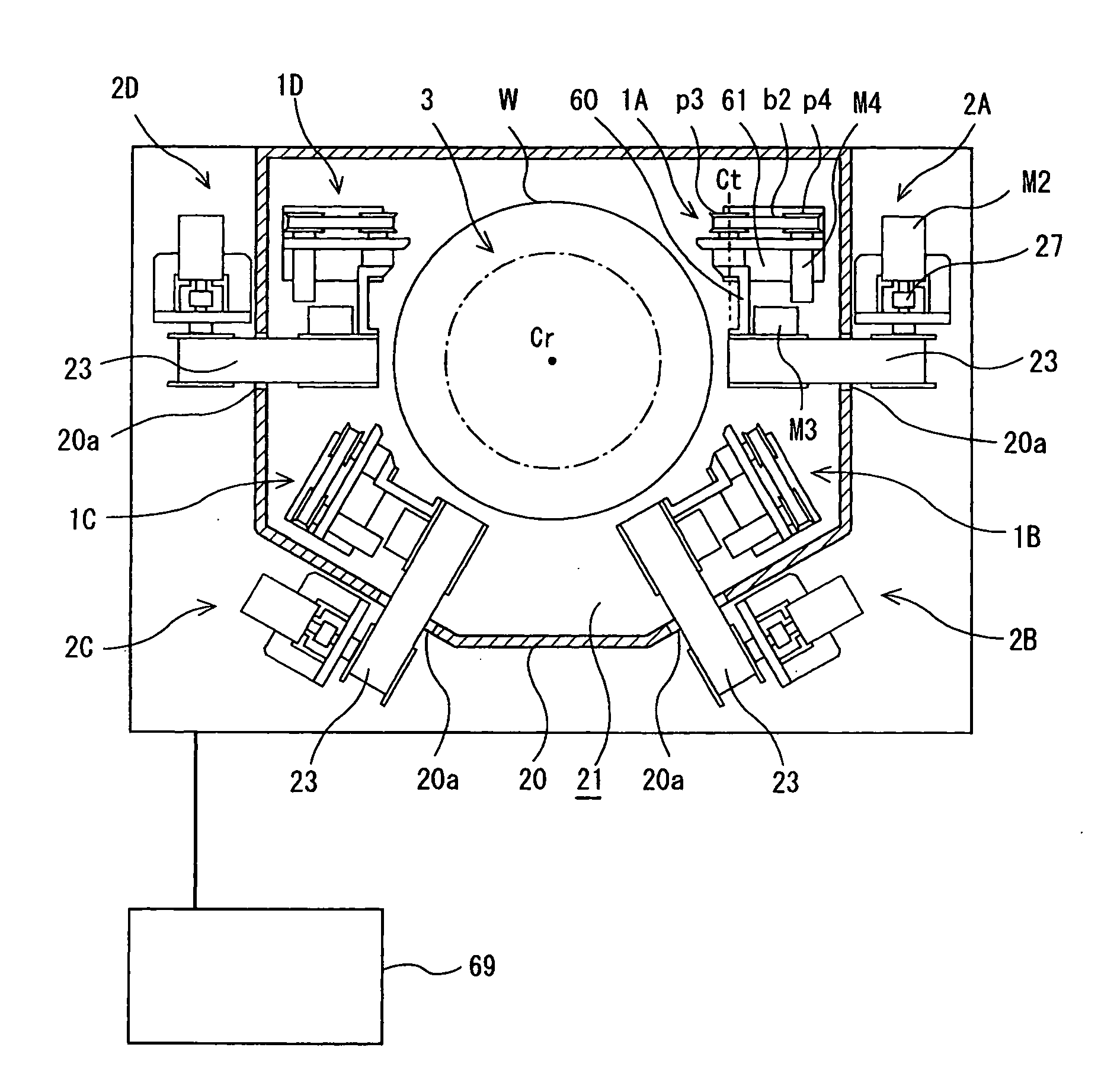
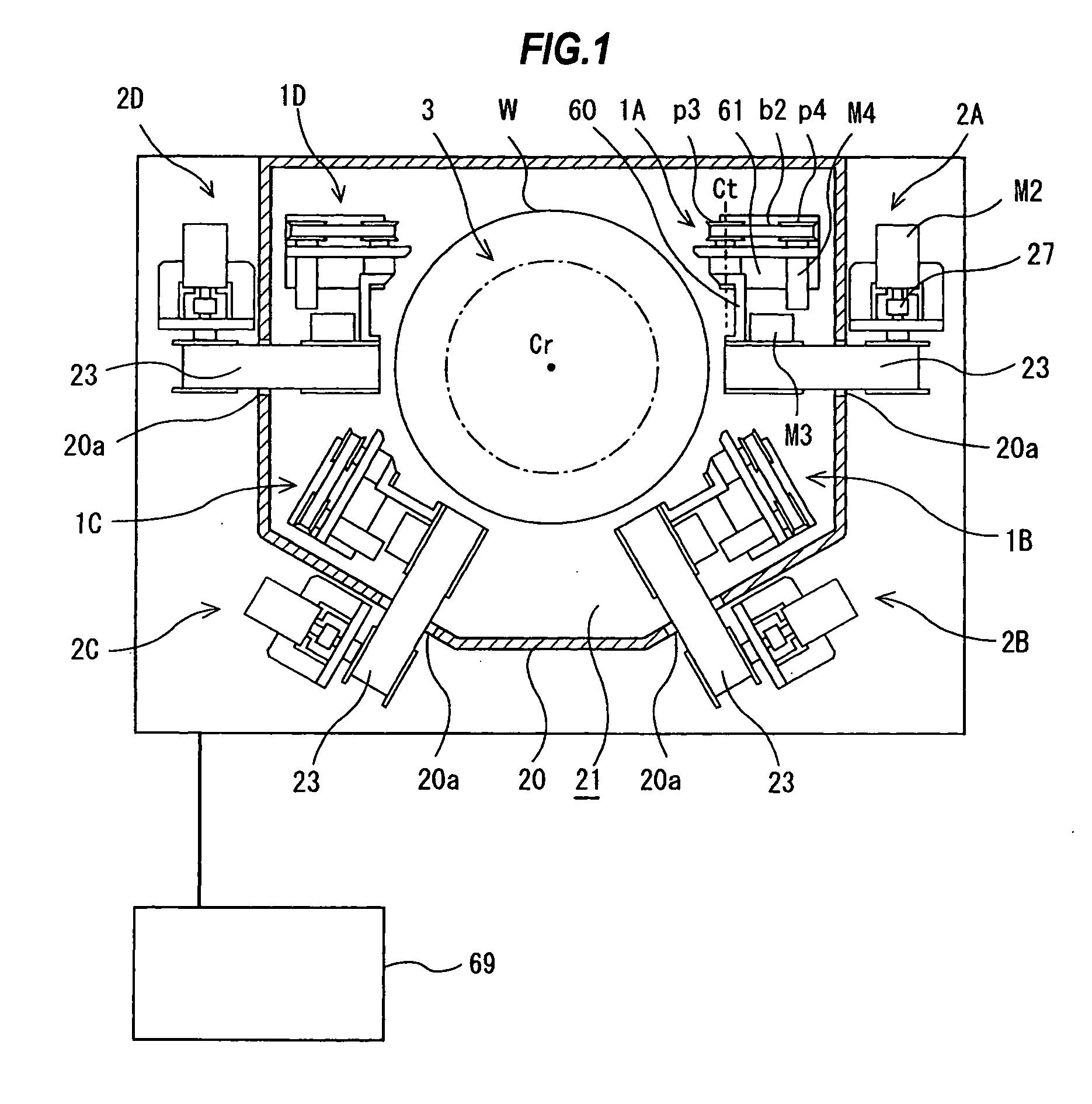
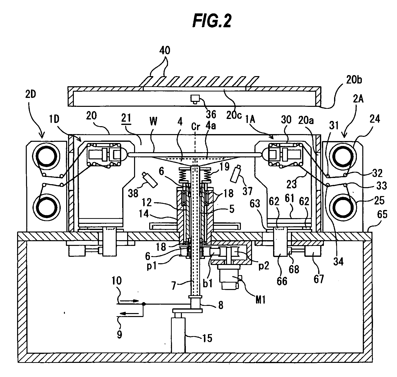
[0136]FIG. 14 is a plan view showing a polishing apparatus according to the second embodiment of the present invention. FIG. 15 is a cross-sectional view taken along line A-A in FIG. 14. FIG. 16 is a side view of the polishing apparatus as viewed from a direction indicated by arrow B in FIG. 14. FIG. 17 is a cross-sectional view taken along line C-C in FIG. 14. Elements that are identical or similar to those of the first embodiment are denoted by the same reference numerals, and will not be described repetitively. In addition, structures and operations of this embodiment, which will not be described below, are the same as those of the first embodiment described above.

[0137]The polishing apparatus according to this embodiment is suitable for use in polishing of a notch portion formed in a periphery of a wafer W. As shown in FIG. 14, this polishing apparatus includes two polishing head modules 70A and 70B, and rotary holding mechanis...

third embodiment

[0170]FIG. 24 is a plan view showing another example of the polishing apparatus according to the present invention. As shown in FIG. 24, in this example, two polishing head modules 70C and 70D are provided in addition to the two polishing head modules 70A and 70B in FIG. 22. These polishing head modules 70C and 70D have the same structure as the polishing head modules 70A and 70B. The polishing head modules 70A and 70B are movable by the linear moving mechanisms in the directions toward and away from the notch portion of the wafer W, as indicated by arrows.

[0171]FIG. 25 is a plan view showing a polishing apparatus according to a fourth embodiment of the present invention, and FIG. 26 is a cross-sectional view taken along line F-F in FIG. 25. The polishing apparatus according to the fourth embodiment is suitable for use in polishing of the bevel portion of the substrate. As shown in FIG. 25, the polishing apparatus according to this embodiment has five polishing head assemblies 1A, 1...


PUM

PropertyMeasurementUnit
Temperatureaaaaaaaaaa
Angleaaaaaaaaaa
Speedaaaaaaaaaa

Abstract

The present invention provides a polishing apparatus for polishing a periphery of a substrate. This polishing apparatus includes a rotary holding mechanism configured to hold the substrate horizontally and rotate the substrate, plural polishing head assemblies provided around the substrate, plural tape supplying and recovering mechanisms configured to supply polishing tapes to the plural polishing head assemblies and recover the polishing tapes from the plural polishing head assemblies, and plural moving mechanisms configured to move the plural polishing head assemblies in radial directions of the substrate held by the rotary holding mechanism. The tape supplying and recovering mechanisms are located outwardly of the plural polishing head assemblies in the radial directions of the substrate, and the tape supplying and recovering mechanisms are fixed in position.

Description

BACKGROUND OF THE INVENTION[0001]1. Field of the Invention[0002]The present invention relates to a polishing apparatus and a polishing method for polishing a substrate such as a semiconductor wafer, and more particularly to a polishing apparatus suitable for use as a bevel polishing apparatus for polishing a bevel portion of a substrate and as a notch polishing apparatus for polishing a notch portion of a substrate.[0003]2. Description of the Related Art[0004]From a viewpoint of improving a yield in semiconductor fabrications, management of a surface condition in a periphery of a semiconductor wafer has recently been drawing attention. In semiconductor fabrication processes, a number of materials are deposited on a wafer repeatedly to form multilayer structures. As a result, unwanted films and a roughened surface are formed on a periphery of the wafer which is not used for products. In recent years, it has become more common to transfer the wafer by holding only the periphery of the...

Claims


Application Information

Patent Timeline
IPC IPC(8): B24B1/00B24B9/00B24B21/00B24B37/00B24B37/04H01L21/304
CPCB24B9/065B24B37/30B24B37/042B24B21/002B24B21/008B24B21/18B24B21/20B24B21/004B24B27/0076B24B41/068B24B49/00Y10T428/24777B24B21/00H01L21/304
Inventor TAKAHASHI, TAMAMISEKI, MASAYAKUSA, HIROAKIYAMAGUCHI, KENJINAKANISHI, MASAYUKI
Owner EBARA CORP
Why Eureka
Try Eureka