Method for manufacturing an eeprom cell

a technology of eeprom cell and manufacturing method, which is applied in the direction of electrical equipment, semiconductor devices, instruments, etc., can solve the problems of leakage of charges stored in the floating gate of the storage element, and not desirable, and achieve the effect of improving the charge retention in the floating ga

Active Publication Date: 2009-06-11
STMICROELECTRONICS (ROUSSET) SAS
View PDF4 Cites 7 Cited by
  • Summary
  • Abstract
  • Description
  • Claims
  • Application Information

AI Technical Summary

Benefits of technology

[0010]An aspect of the present invention aims at a method for manufacturing an EEPROM cell which enables improving the

Problems solved by technology

A disadvantage of a conventional EEPROM cell is that a leakage of the charges stored in the floating gate of the storage element, which tend to e

Method used


Image

  • Method for manufacturing an eeprom cell
  • Method for manufacturing an eeprom cell
  • Method for manufacturing an eeprom cell

Examples


Embodiment Construction

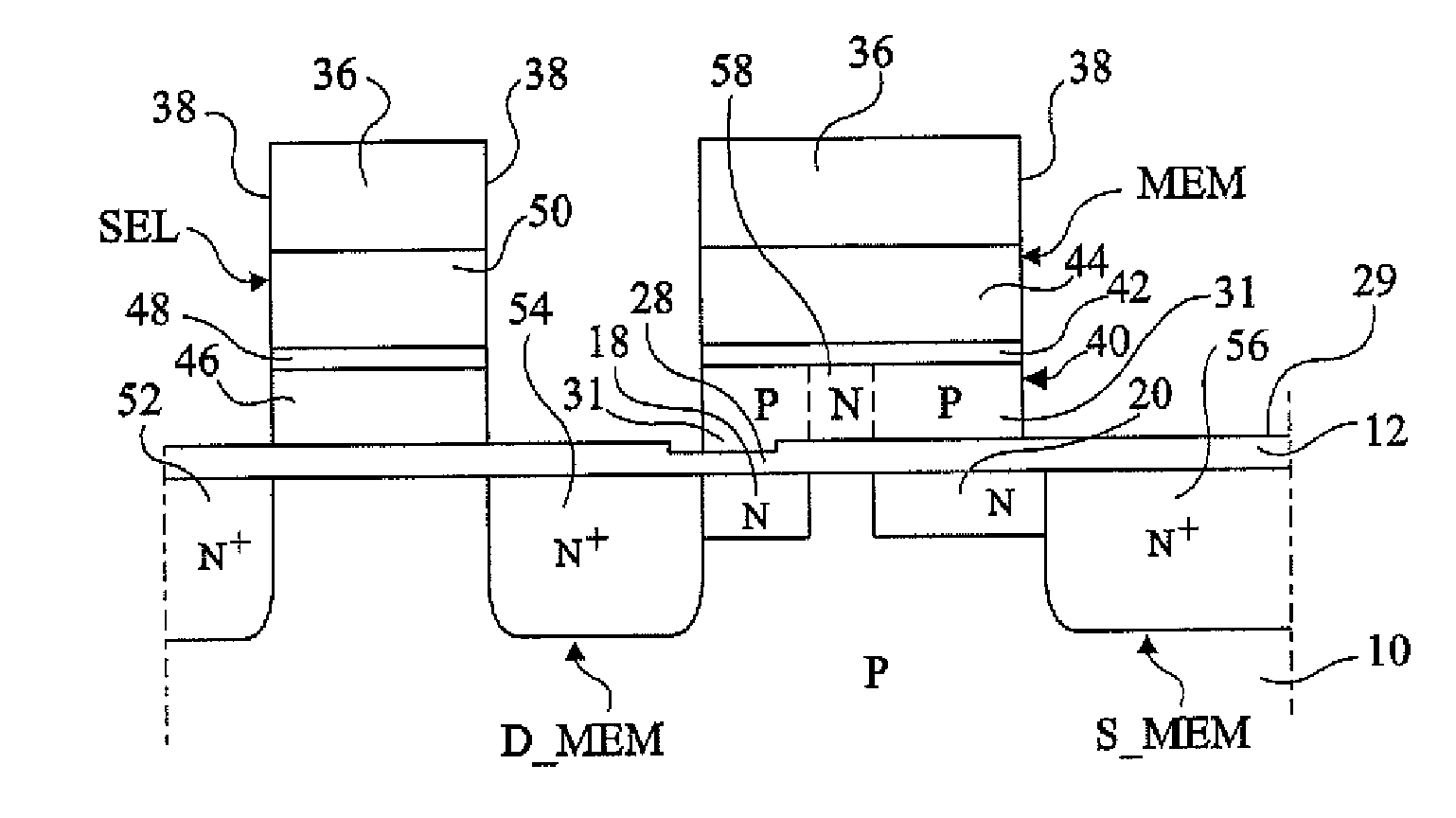
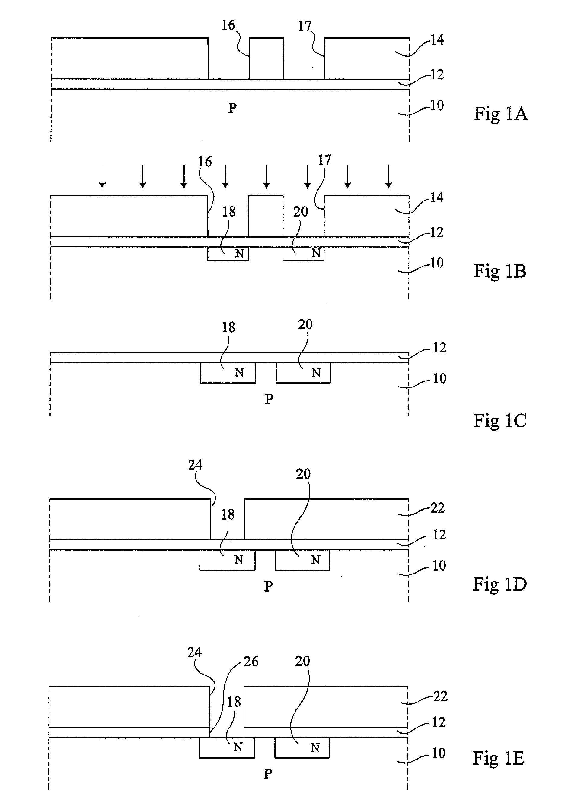
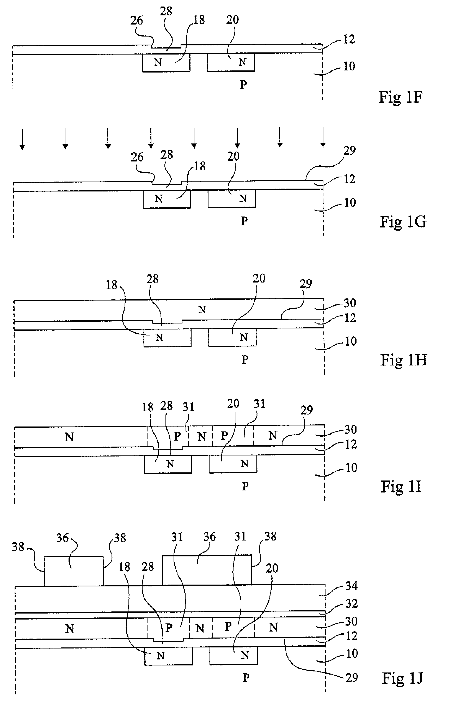
[0031]For clarity, the same elements have been designated with the same reference numerals in the different drawings and, further, as usual in the representation of integrated circuits, the various drawings are not to scale.

[0032]To prevent the diffusion of P-type dopant elements in the EEPROM cell substrate in the step of forming, by implantation, of P-type doped regions in the floating gate of the EEPROM cell storage element, the applicant has first tried to use a method similar to that implemented in CMOS manufacturing processes. Indeed, in manufacturing of conventional P-channel MOS transistors, the transistor gate is generally doped by implantation of P-type dopant elements. To prevent the diffusion of the dopant elements of the transistor gate into the underlying substrate, a nitrided oxide which is obtained by growing a silicon oxide layer under a nitrogen flow (in the form of nitrogen oxide NO or of nitrogen dioxide NO2) is used as a gate insulator.

[0033]The floating gate in...


PUM


Abstract

A method for manufacturing a cell of a non-volatile electrically erasable and programmable memory including a dual-gate MOS transistor. The method includes the steps of providing a semiconductor substrate covered with an insulating layer including a thinned down portion and having a first surface common with the substrate and a second surface opposite to the first surface; and incorporating nitrogen at the level of the second surface, whereby the maximum nitrogen concentration is closer to the second surface than to the first surface.

Description

CROSS REFERENCE TO RELATED APPLICATIONS[0001]This application claims the priority benefit of French patent application Ser. No. 07 / 59563, filed on Dec. 5, 2007, entitled “Method for Manufacturing an Eeprom Cell,” which is hereby incorporated by reference to the maximum extent allowable by law.BACKGROUND OF THE INVENTION[0002]1. Field of the Invention[0003]The present invention relates to methods for manufacturing cells of an electrically erasable and programmable non-volatile memory or EEPROM cells and to the memory cells obtained with such methods.[0004]2. Discussion of the Related Art[0005]An EEPROM cell generally comprises a selection element and a storage element. As an example, the selection element corresponds to a conventional single-gate MOS transistor and the storage element corresponds to a dual-gate MOS transistor comprising a floating gate covered with a control gate. The floating gate insulator comprises a thinned portion at the level of the dual-gate transistor drain w...

Claims


Application Information

Patent Timeline
IPC IPC(8): H01L29/78H01L29/68H01L21/336
CPCH01L27/115H01L27/11521H01L29/7883H01L29/42324H01L27/11524H10B41/35H10B69/00H10B41/30
Inventor FORNARA, PASCAL
Owner STMICROELECTRONICS (ROUSSET) SAS
Why Eureka
Try Eureka