Semiconductor device

a technology of semiconductors and shields, applied in the direction of semiconductor devices, semiconductor/solid-state device testing/measurement, semiconductor/solid-state device details, etc., can solve the problems of increasing the number of times electrode pad probing is carried out, increasing contact damage due to the probe needle, and reducing the chip size. , to ensure bonding reliability, prevent damage to the esd protection device, the effect of reducing the chip siz

Inactive Publication Date: 2009-06-11
ELPIDA MEMORY INC
View PDF5 Cites 5 Cited by
  • Summary
  • Abstract
  • Description
  • Claims
  • Application Information

AI Technical Summary

Benefits of technology

[0028]According to the present invention, since the external electrode pad is divided into the bonding area and the probing area, it is possible to ensure bonding reliability, and in addition, since the ESD protection device is arranged below the probing area, it is possible to reduce chip size, in comparison to cases in which the ESD protection device is not arranged below the external electrode pad.
[0029]In addition, since the load on the probing area wh...

Problems solved by technology

In the semiconductor devices of Patent Document 1 through Patent Document 3, one electrode pad is a bonding target, and also a probing target; however, in these semiconductor devices, there is a risk of a contact defect occurring when bonding is carried out, that is, a risk of bonding reliability decreasing, due to damage by the probe needle as indicated in Patent Document 4.
Therefore, in MobileRAM and the like, the number of times probing is carried out on the electrode pad increases, and contact damage due to the probe needle also increases.
The increase in contact damage due to the probe needle in the electrode pad causes effective contact area of the bonding wire and the electrode pad to decrease when bonding is carried out, and as a result, there is a possibility that the bonding reliability will decrea...

Method used


Image

  • Semiconductor device
  • Semiconductor device
  • Semiconductor device

Examples


first exemplary embodiment

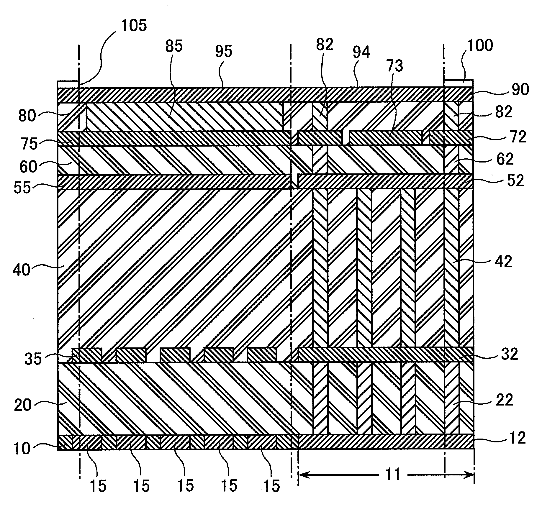
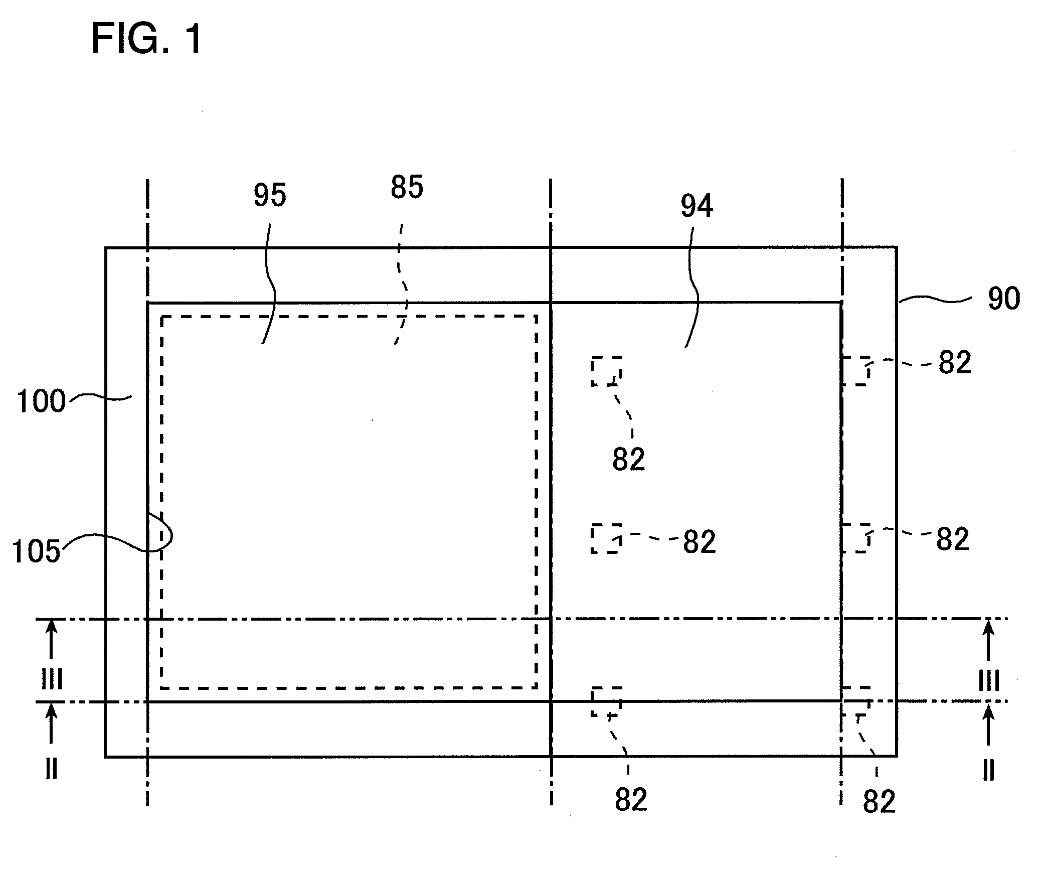
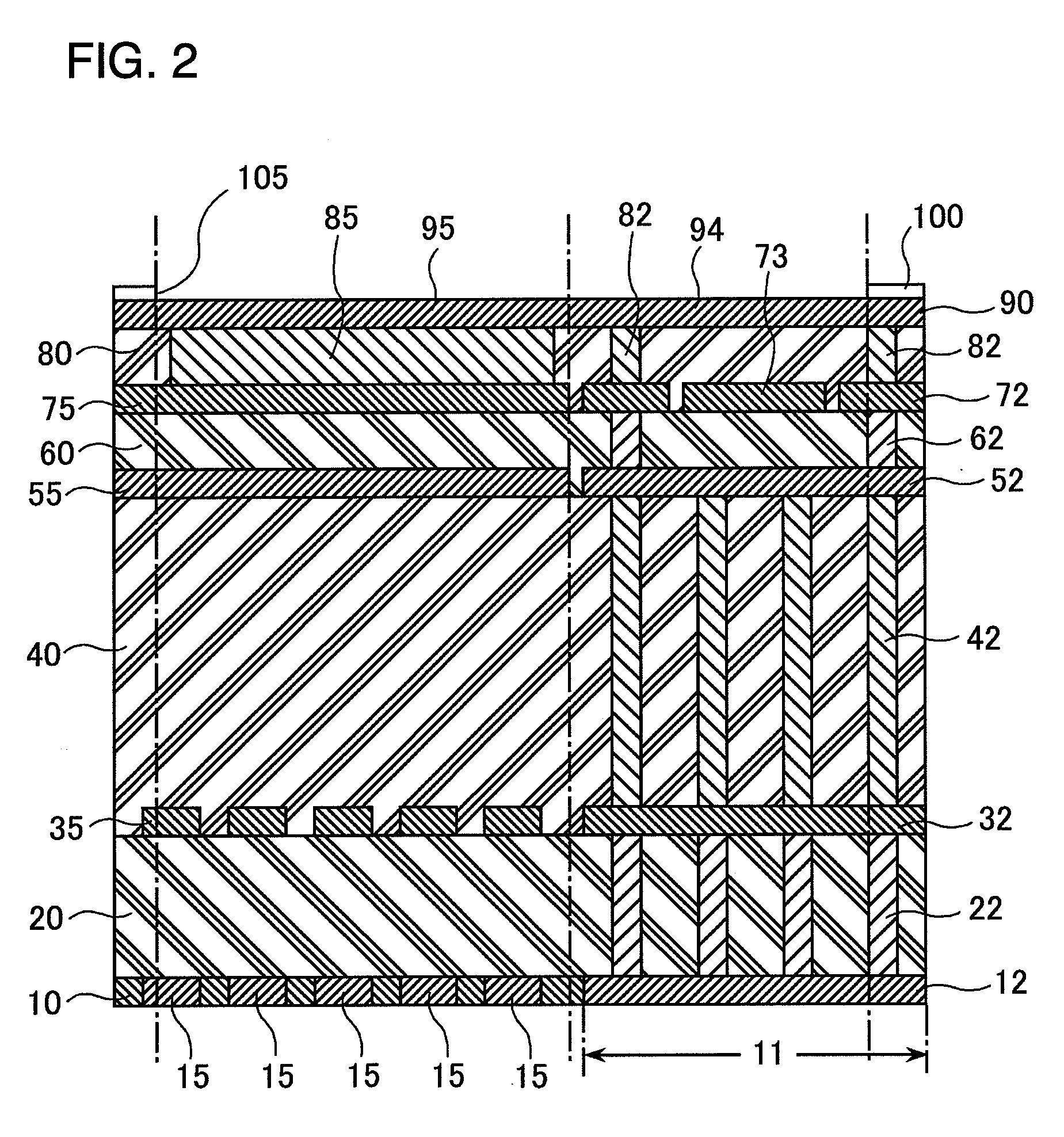
[0043]A semiconductor device according to a first exemplary embodiment of the present invention, as shown in FIG. 1 through FIG. 6, has four metal layers and is provided with an external electrode pad 90 in the fourth layer (uppermost layer). In outline, the external electrode pad 90 in the present exemplary embodiment, to avoid a bonding defect arising from contact damage of a probe needle when probing is carried out, separately has a bonding area 95, which is an area for wire bonding, and a probing area 94, which is an area to which the probe needle is applied when probing is carried out, and an ESD protection device is provided below the probing area 94.

[0044]In detail, as shown in FIG. 2 and FIG. 3, the semiconductor device according to the present exemplary embodiment has a substrate 10. The substrate 10 is provided with a protection device region 11 forming an ESD protection device; and diffusion regions being a drain region 12 and a source region 13 of the ESD protection devi...

second exemplary embodiment

[0056]A semiconductor device according to a second exemplary embodiment of the present invention is a modified example of the first exemplary embodiment as described above, and concretely, by having an opening of a polyimide film, formed on an external electrode pad, in a specific shape, the opening of the polyimide film has a function as a marker, enabling a bonding area and a probing area to be distinguished, when the external electrode pad is viewed from above. In the following, only points of difference from the semiconductor device according to the first exemplary embodiment are described, and descriptions of other points are omitted.

[0057]The semiconductor device according to the present exemplary embodiment is provided with the polyimide film 100b that has the opening 105b as shown in FIG. 9. Specifically, by making the opening width of the opening 105b different for the bonding area 95b and the probing area 94b, a step 107b is formed at a boundary portion of the bonding area...

third exemplary embodiment

[0059]A semiconductor device according to a third exemplary embodiment of the present invention is a modified example of the first exemplary embodiment similar to the second exemplary embodiment, and concretely, by making an opening of a polyimide film, formed on the external electrode pad, in a specific shape, the opening of the polyimide film has a function as a marker, enabling the bonding area and the probing area to be distinguished, when the external electrode pad is viewed from above. In the following, only points of difference from the semiconductor device according to the first exemplary embodiment are described, and descriptions of other points are omitted.

[0060]The semiconductor device according to the present exemplary embodiment is provided with a polyimide film 100c that has an opening 105c as shown in FIG. 11. Specifically, at a position equivalent to a boundary portion of a bonding area 95c and a probing area 94c, protruding parts 107c, protruding so as to face each ...


PUM


Abstract

A semiconductor device which can prevent damage to an ESD protection device by pressure when bonding is carried out, while having a pad configuration that can ensure bonding reliability, with the semiconductor device being made as small as possible. A bonding area that is an area for wire bonding with respect to an external electrode pad and a probing area that is an area in which a probe needle is applied when probing, are provided, and the ESD protection device and a discharge path therefor are arranged below the probing area. Arranged below the bonding area are a support via that is a little smaller than the bonding pad, and a support pattern having a size corresponding to the bonding pad and joined to the bonding pad by the support via.

Description

REFERENCE TO RELATED APPLICATION[0001]This application is based upon and claims the benefit of the priority of Japanese patent application No. 2007-315943, filed on Dec. 6, 2007, the disclosure of which is incorporated herein in its entirety by reference thereto.BACKGROUND OF THE INVENTION[0002]1. Field of the Invention[0003]The present invention relates to a semiconductor device provided with an ESD protection device for preventing damage to an internal element due to electrostatic noise incoming from an external electrode pad.[0004]2. Description of Related Art[0005]Conventionally, in order to reduce the size of a semiconductor device provided with an ESD protection device, technology is proposed in which the ESD protection device is formed below a bonding pad (for example, refer to Patent Documents 1 through 3).[0006]Moreover, although not related to a semiconductor device that has a pad electrode, there is a proposal of a structure which considers as a problem, damage produced b...

Claims


Application Information

Patent Timeline
IPC IPC(8): H01L23/495
CPCH01L22/32H01L23/60H01L24/05H01L27/0203H01L2224/02166H01L2224/05553H01L2924/01004H01L2924/01006H01L2924/01033H01L27/0248
Inventor ONDA, TAKAMITSUMATSUKI, KAZUHIKO
Owner ELPIDA MEMORY INC
Why Eureka
Try Eureka