Magnetic field detector
a magnetic field and detector technology, applied in the direction of magnetic property measurement, electrical apparatus, semiconductor devices, etc., can solve the problems of stray field, leakage of magnetic field to the outside of the element, mutual interference, etc., to improve the performance of a magnetic field detector, and achieve high-density magnetic field
- Summary
- Abstract
- Description
- Claims
- Application Information
AI Technical Summary
Benefits of technology
Problems solved by technology
Method used
Image

Examples
first embodiment
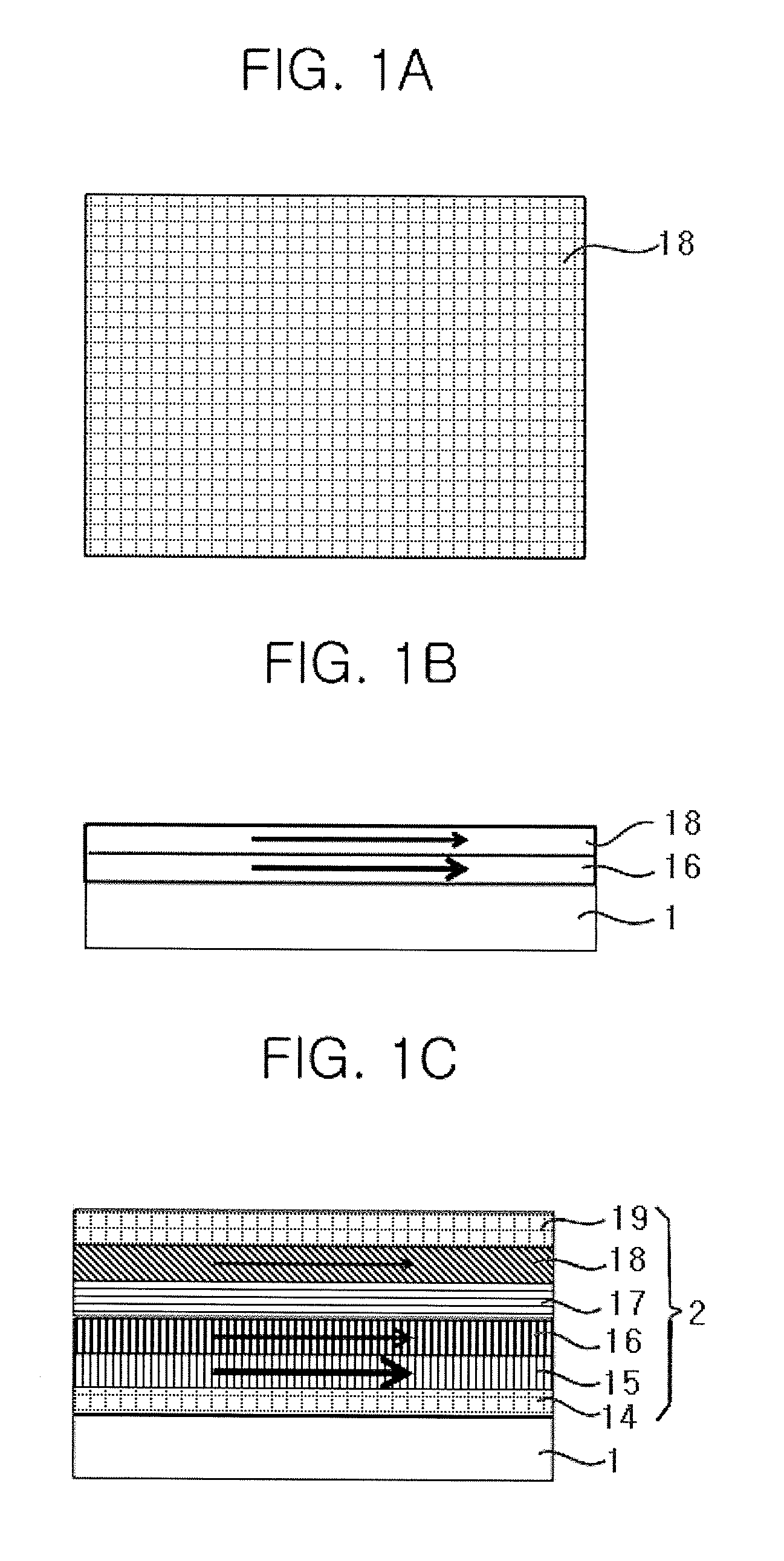
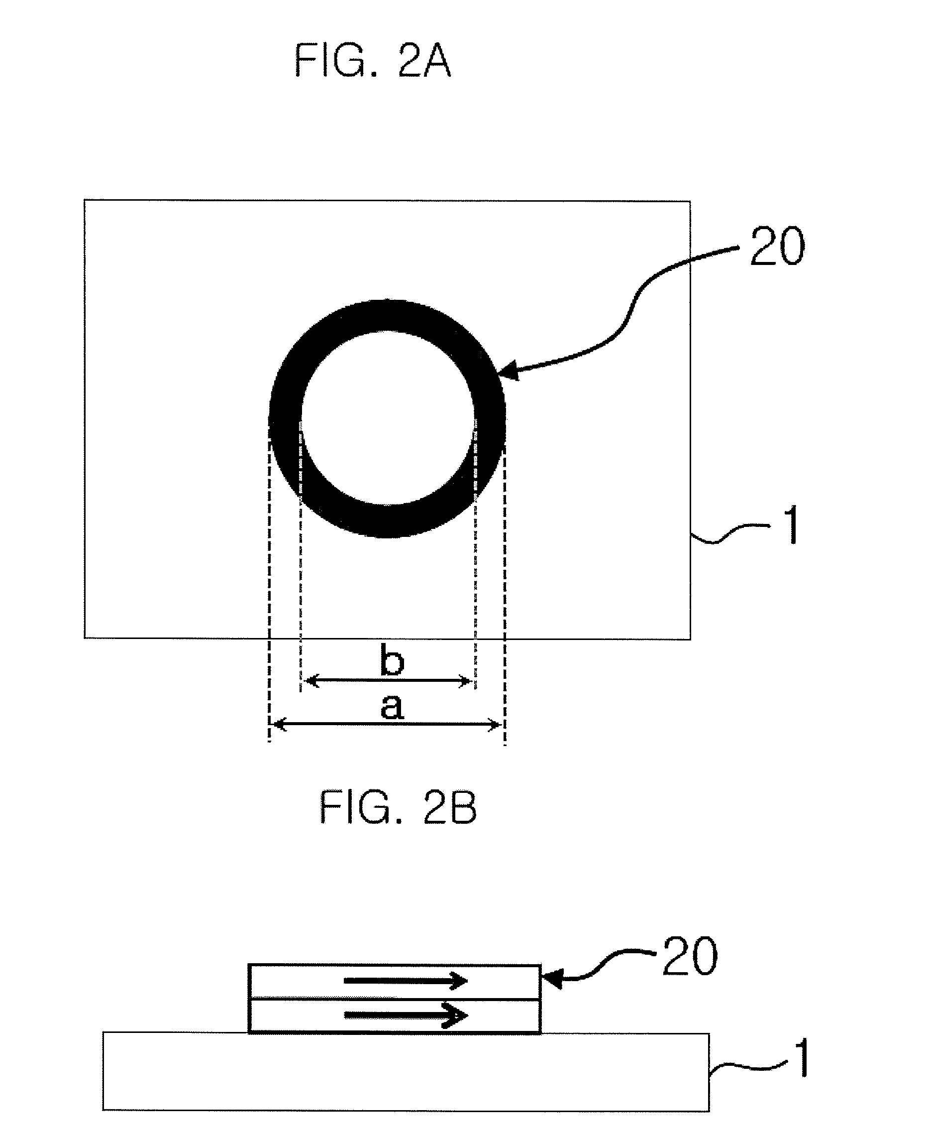
[0069]FIGS. 2A to 8B are diagrams sequentially illustrating the structure of a magnetic field detector according to a first embodiment of the invention and a method of manufacturing the same. The magnetic field detector according to the first embodiment is characterized in that it includes a magnetoresistive element with a single circular ring shape.
[0070]First, the giant magnetoresistive thin film 2 is formed on the substrate 1 by vapor deposition and then etched to form a magnetoresistive element 20 with a circular ring shape (see FIGS. 2A and 2B). In the etching process, dry etching, such as an Ar gas ion milling method, is performed on the giant magnetoresistive thin film 2 shown in FIG. 1C to etch all the portions of the film except a circular ring portion. FIG. 2A is a plan view, and FIG. 2B is a diagram illustrating the arrangement of the substrate 1 and the magnetoresistive element 20. For example, in the first embodiment, the magnetoresistive element 20 has an outside diame...
second embodiment
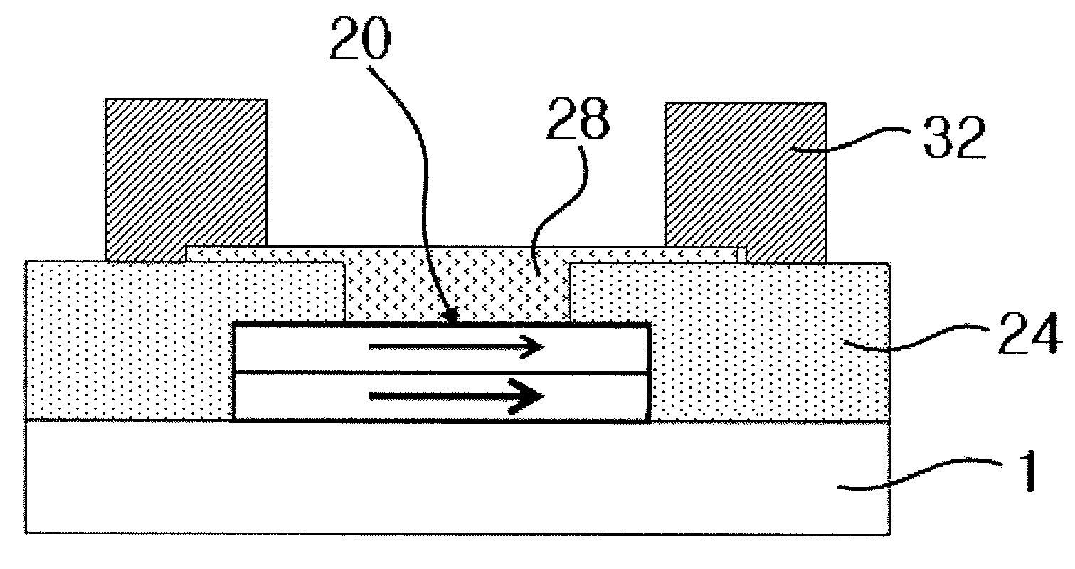
[0081]FIGS. 10A to 16B are diagrams sequentially illustrating the structure of a magnetic field detector according to a second embodiment of the invention and a method of manufacturing the same. The magnetic field detector according to the second embodiment differs from the magnetic field detector according to the first embodiment in that it further includes vertical electrodes (vertical electrode pads).
[0082]First, a giant magnetoresistive thin film 2 is formed on a substrate 1 by vapor deposition and then etched to form a magnetoresistive element 20 with a circular ring shape (see FIGS. 10A and 10B). In the etching process, dry etching, such as an Ar gas ion milling method, is performed on the giant magnetoresistive thin film 2 shown in FIG. 1C to etch all the portions of the film except a circular ring portion. FIG. 10A is a plan view, and FIG. 10B is a diagram illustrating the arrangement of the substrate 1 and the magnetoresistive element 20.
[0083]As shown in FIGS. 11A and 11B,...
third embodiment
[0092]FIGS. 17A to 23B are diagrams sequentially illustrating the structure of a magnetic field detector according to a third embodiment of the invention and a method of manufacturing the same. The third embodiment differs from the first embodiment in that a plurality of magnetoresistive elements having circular ring shapes (that is, a one-dimensional array structure) are arranged in a line. Since the manufacturing method according to the third embodiment is most similar to that according to the first embodiment, those skilled in the art can easily understand the manufacturing method according to the third embodiment.
[0093]First, a giant magnetoresistive thin film 2 is formed on a substrate 1 by vapor deposition and then etched to form an array of a plurality of magnetoresistive elements 20 with circular ring shapes (see FIGS. 17A and 17B). The plurality of magnetoresistive elements 20 are arrayed in a line at equal distances. In the etching process, dry etching, such as an Ar gas i...
PUM
 Abstract
Description
Claims
Application Information
 - R&D
- Intellectual Property
- Life Sciences
- Materials
- Tech Scout
- Unparalleled Data Quality
- Higher Quality Content
- 60% Fewer Hallucinations
Browse by: Latest US Patents, China's latest patents, Technical Efficacy Thesaurus, Application Domain, Technology Topic, Popular Technical Reports.
© 2025 PatSnap. All rights reserved.Legal|Privacy policy|Modern Slavery Act Transparency Statement|Sitemap|About US| Contact US: help@patsnap.com