Piezoelectric oscillator and method for manufacturing the same

a technology of piezoelectric oscillator and piezoelectric resonator, which is applied in the direction of generator/motor, piezoelectric/electrostrictive transducer, transducer type, etc., can solve the problems of reducing the reliability of the electrical coupling between the ic chip and the piezoelectric resonator, and the problem becomes more significant, so as to improve the reliability of the electrical coupling and reduce the mounting area.

Inactive Publication Date: 2009-06-18
SEIKO EPSON CORP
View PDF5 Cites 11 Cited by
  • Summary
  • Abstract
  • Description
  • Claims
  • Application Information

AI Technical Summary

Benefits of technology

[0008]An advantage of the invention is to provide a piezoelectric oscillator that is downsized so that the mount area thereof is reduced and whose reliability with respect to the electrical coupling is improved, and a method for manufacturing the piezoelectric oscillator.
[0009]A piezoelectric oscillator according to a first aspect of the invention includes: a piezoelectric resonator including a container, the container containing a piezoelectric resonator element; and a semiconductor device including an oscillation circuit for vibrating the piezoelectric resonator. The semiconductor device is bonded to a surface of the container. The container has an external coupling terminal and a cut-off part, the external coupling terminal being coupled to the semiconductor device, the cut-off part being disposed on a side surface of the container. The external coupling terminal is disposed in an area of the container, the area being opposed to the semiconductor device, and in the cut-off part. The semiconductor device has a coupling terminal on a surface thereof, the surface being opposed to the container. The coupling terminal of the semiconductor device and the external coupling terminal of the container are coupled with a conductive material.
[0010]By adopting the above-mentioned configuration, the semiconductor device is disposed on and bonded to the piezoelectric resonator. Thus, the piezoelectric oscillator as a whole is made compact.
[0011]Also, the container of the piezoelectric resonator has the external coupling terminal for coupling the container to the semiconductor device. This external coupling terminal is disposed in an area of the container that is opposed to the semiconductor device when the semiconductor device is bonded to the container, and is also disposed in the cut-off part connected to the area and formed on the outer surface of the container.
[0012]Thus, when solder or a conductive adhesive for bonding is applied to the external coupling terminal of the container, the solder or conductive adhesive extends to the cut-off part, that is, a castellation so that a solder fillet or the like is formed. As a result, the bonding between the container of the piezoelectric resonator element and semiconductor device is strengthened so that the electrical coupling therebetween is ensured.
[0013]In the piezoelectric oscillator according to the first aspect of the invention, the container preferably may have a plurality of the external coupling terminal and a concave part is preferably provided between the external coupling terminals in the area of the container.

Problems solved by technology

Accordingly, there occurs a problem that the reliability with respect to the electrical coupling between the IC chip and piezoelectric resonator is reduced.
This problem becomes more significant as the IC chip and piezoelectric resonator are made smaller.

Method used


Image

  • Piezoelectric oscillator and method for manufacturing the same
  • Piezoelectric oscillator and method for manufacturing the same
  • Piezoelectric oscillator and method for manufacturing the same

Examples


first embodiment

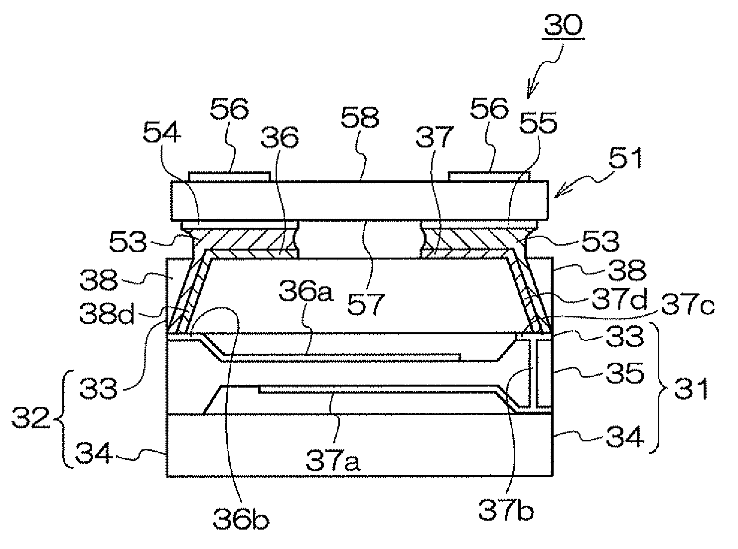
[0036]FIG. 1 is a schematic sectional view showing a piezoelectric oscillator according to the invention. FIG. 2 is a top view (plan view) of a package serving as a container. As shown in FIG. 1, a piezoelectric oscillator 30 is formed by bonding together a piezoelectric resonator 31 and a semiconductor device 51 including an oscillation circuit for vibrating a piezoelectric resonator element 35 contained in a package 32 of the piezoelectric resonator 31.

[0037]As shown in FIG. 1, the piezoelectric resonator 31 according to this embodiment includes the package 32 including first and second substrates 33 and 34 and serving as a container, and the piezoelectric resonator element 35 interposed and fixed between these substrates.

[0038]The first and second substrates 33 and 34 are preferably light-transmissive, flat plates that are made of glass, more preferably, a material identical to that of the piezoelectric resonator element 35. In other words, the first and second substrates 33 and ...

second embodiment

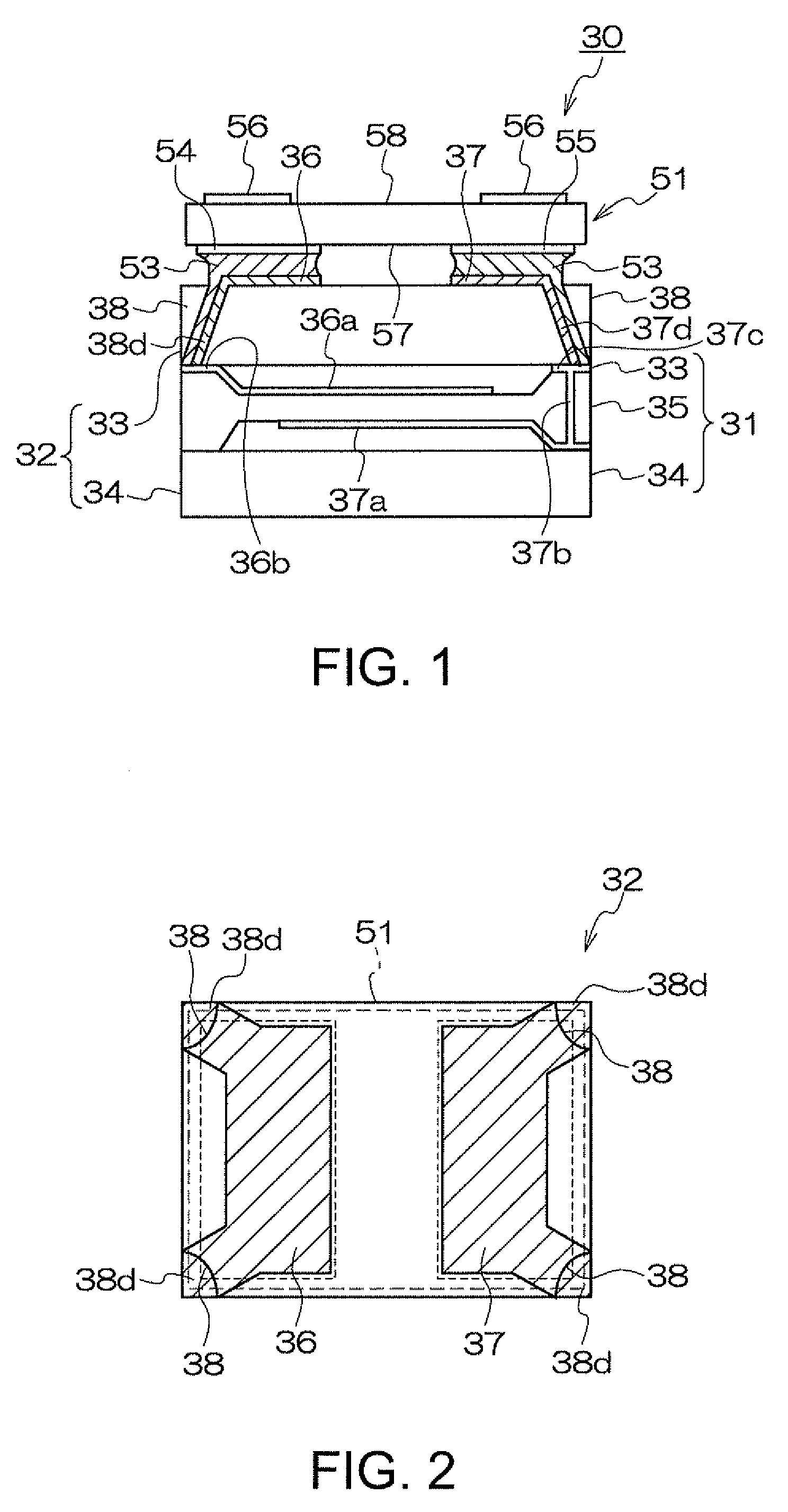
[0059]FIG. 3 is a schematic sectional view showing a piezoelectric oscillator according to the invention. Elements common to FIG. 3 and FIGS. 1 and 2 are assigned same reference numerals and will not be described again. The difference between these drawings will be mainly described.

[0060]The difference between a piezoelectric oscillator 30-2 according to this embodiment and the piezoelectric oscillator 30 according to the first embodiment is the configuration of a semiconductor device 51-2. As shown in FIG. 3, the outer surface of the semiconductor device 51-2 according to this embodiment is a slope 51a that is gradually inclined inwardly of the semiconductor apparatus as the slope descends.

[0061]The piezoelectric oscillator according to this embodiment is configured as described above. Since the outer surface of the semiconductor device 51-2 is the slope 51a, the areas of the semiconductor device 51-2 that are bonded to a conductive adhesive or the pieces of solder 53 are increased...

third embodiment

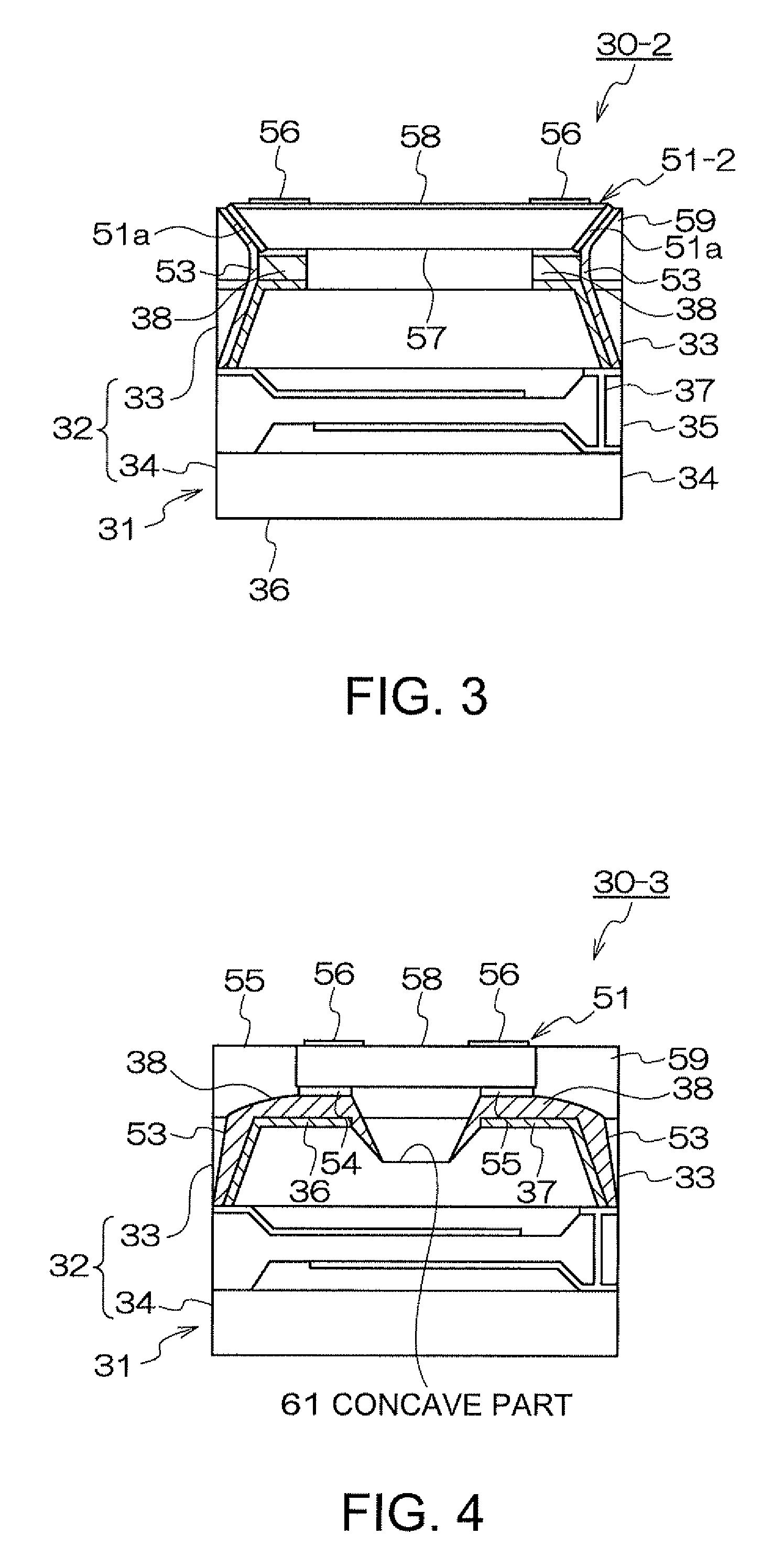
[0062]FIG. 4 is a schematic sectional view showing a piezoelectric oscillator according to the invention. FIGS. 5 and 6 are top views of a package serving as a container of a piezoelectric resonator. Elements common to FIGS. 4 to 6 and FIGS. 1 and 2 are assigned same reference numerals and will not be described again. The difference between these drawings will be mainly described.

[0063]This embodiment is an example in which the external dimensions of a semiconductor device are made smaller than those of the package.

[0064]In this embodiment, a concave part 61 is provided between the external coupling terminals 36 and 37 that are multiple external coupling terminals provided on the first substrate 33 of the package 32. The concave part 61 is formed on the upper surface of the first substrate 33 opposed to the semiconductor device 51. FIG. 5 shows a top view (plan view) of the package 32. The concave part 61 may take various forms. In this embodiment, the concave part 61 is a groove ex...


PUM

PropertyMeasurementUnit
areaaaaaaaaaaa
conductiveaaaaaaaaaa
piezoelectricaaaaaaaaaa

Abstract

A piezoelectric oscillator includes: a piezoelectric resonator including a container, the container containing a piezoelectric resonator element: and a semiconductor device including an oscillation circuit for vibrating the piezoelectric resonator. The semiconductor device is bonded to a surface of the container. The container has an external coupling terminal and a cut-off part, the external coupling terminal being coupled to the semiconductor device, the cut-off part being disposed on a side surface of the container. The external coupling terminal is disposed in an area of the container, the area being opposed to the semiconductor device, and in the cut-off part. The semiconductor device has a coupling terminal on a surface thereof, the surface being opposed to the container. The coupling terminal of the semiconductor device and the external coupling terminal of the container are coupled with a conductive material.

Description

BACKGROUND[0001]1. Technical Field[0002]The present invention relates to improvements in a piezoelectric oscillator having a structure in which a semiconductor device is bonded to a container of a piezoelectric resonator containing a piezoelectric resonator element, and a method for manufacturing a piezoelectric oscillator.[0003]2. Related Art[0004]A piezoelectric resonator or a piezoelectric oscillator has been widely used in small-size information apparatuses such as hard disk drives (HDDs), mobile computers, and IC cards and mobile communication apparatuses such as cell phones, car phones, and paging systems. A piezoelectric oscillator is formed by bonding together a piezoelectric resonator element made of a piezoelectric material and a semiconductor device, that is, an IC chip.[0005]JP-A-2006-60638 shows an example of a piezoelectric oscillator. In a quartz crystal oscillator shown in FIG. 1 of JP-A-2006-60638, an IC chip 5 is bonded to a mount substrate 2 with a bump 6 therebet...

Claims


Application Information

Patent Timeline
Patent Type & Authority Applications(United States)
IPC IPC(8): H03B5/36H01L41/053H01L41/22
CPCY10T29/42H03B5/36
Inventor MATSUO, ATSUSHI
Owner SEIKO EPSON CORP
Why Eureka
Try Eureka