
Multi-threshold voltage-biased circuits

a voltage biasing and multi-threshold technology, applied in the direction of power consumption reduction, electric pulse generator details, electric variable regulation, etc., can solve the problems of damage to circuit components, limited power resources in electronic devices, and close association of power consumption with heat dissipation in integrated circuits, so as to limit the leakage current

Inactive Publication Date: 2009-06-25
ATI TECH INC
View PDF9 Cites 20 Cited by
  • Summary
  • Abstract
  • Description
  • Claims
  • Application Information

AI Technical Summary

Benefits of technology

[0010]In accordance with one aspect of the present invention there is provided, a method of operating an integrated circuit. The circuit includes at least one p-channel field effect transistor (FET) and an n-channel FET formed in a substrate. Each of the p-channel FET and n-channel FET include a gate, a source, and a drain. At least one of the FETs further includes a back contact in the substrate. The drain of the p-channel FET interconnects the drain of the n-channel FET. The method includes providing a fixed bias voltage to the back contact to bias a body of the FET with the back contact. The method also includes applying a supply voltage independent of the fixed bias voltage to the source of the FET with the back contact at a first voltage level when the circuit is in a normal state. The method also includes applying the supply voltage at a second voltage level when the circuit is in a low power state. The second voltage level is lower than the first level when the FET with the back contact is the p-channel FET and higher than the first level when the FET with the back contact is the n-channel FET. Adjusting the supply voltage helps limit leakage current between the source of the p-channel FET and the source of the n-channel FET.

Problems solved by technology

Power is a limited resource in electronic devices.
Furthermore, power consumption is closely associated with heat dissipation in integrated circuits.
Excessive power consumption and its dissipation in the form of heat may damage circuit components and render electronic devices inoperable.
Dynamic power consumption is caused primarily by switching logic and the associated charging and discharging of capacitors.
In contrast, static power dissipation is primarily caused by leakage current.
Thus static power dissipation may take place even when the inputs to a given circuit may remain unchanged.
In other words, even if a given circuit is not actively switching, static power dissipation takes place as a result of leakage current.
Moreover, a transient voltage at the common input may easily turn on both transistors which would cause current to flow and thereby increase static power dissipation.
Unfortunately, high threshold transistors negatively impact signal propagation in circuits.
High threshold transistors cannot be turned on and off as fast as low threshold devices.
Moreover, the output current of a high-threshold transistor is typically lower than that of a low threshold one, and thus a high threshold transistor takes a longer time to charge up a capacitive load.
However, low threshold transistors tend to suffer from high leakage current and therefore consume relatively large amounts of static power.

Method used


Image

  • Multi-threshold voltage-biased circuits
  • Multi-threshold voltage-biased circuits
  • Multi-threshold voltage-biased circuits

Examples


Embodiment Construction

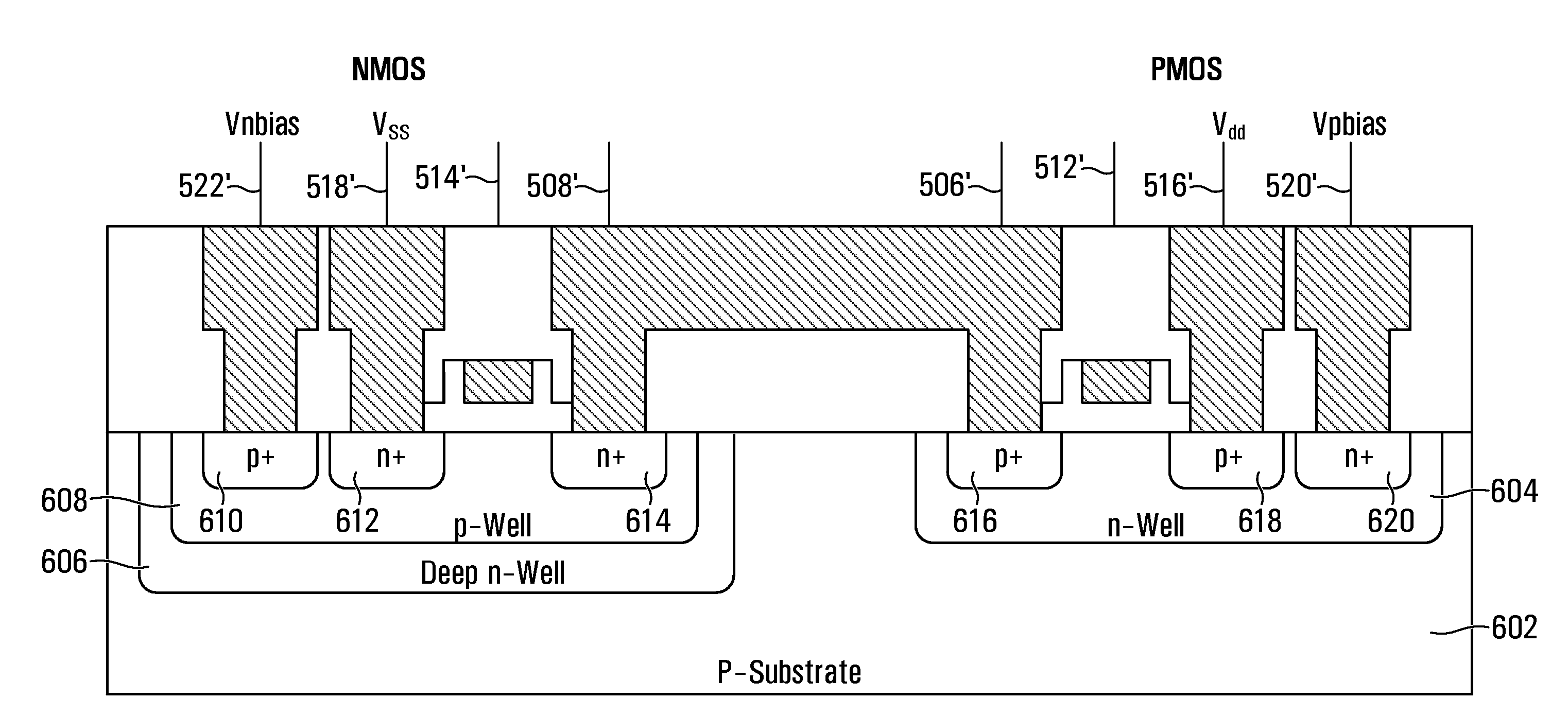
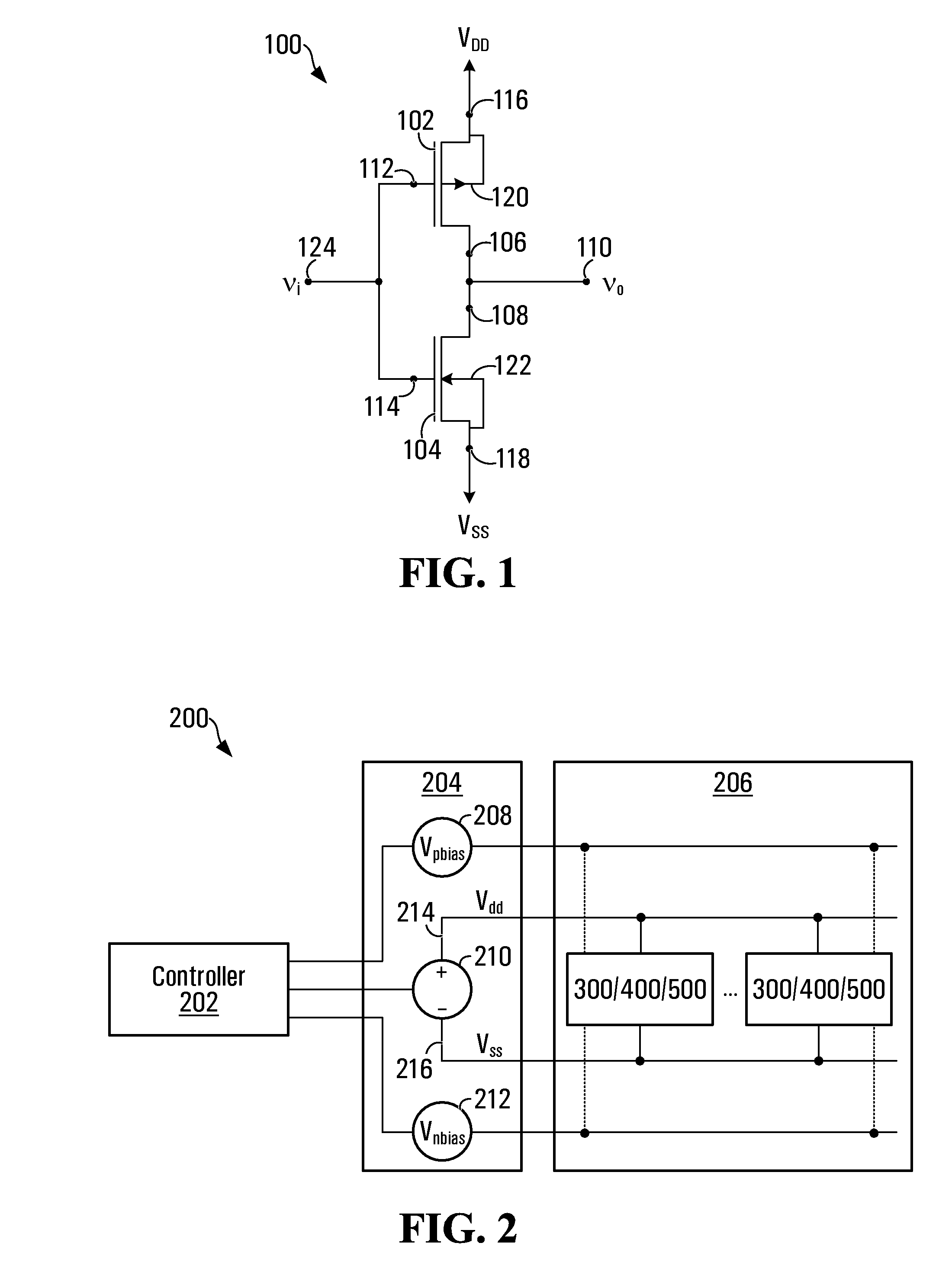
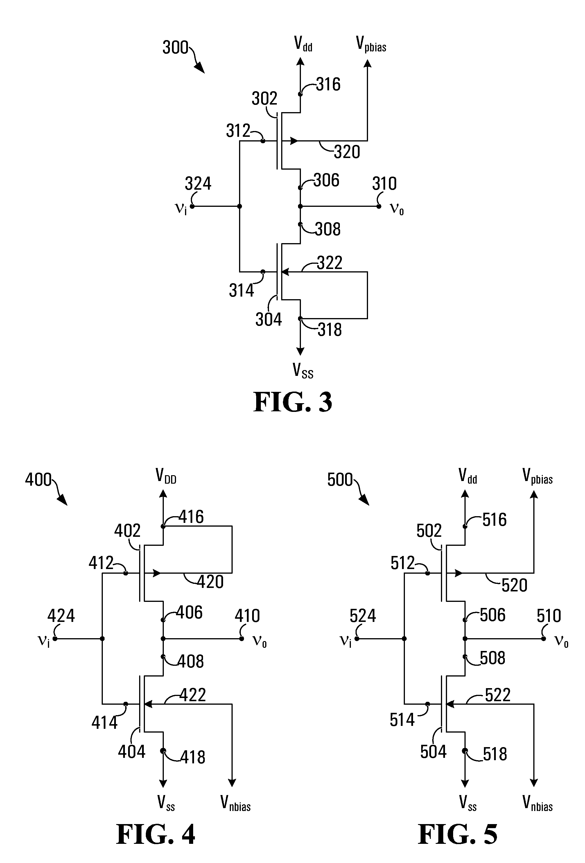
[0023]FIG. 1 is a schematic diagram of a conventional CMOS inverter circuit 100 including a PMOS transistor 102 interconnecting an NMOS transistor 104. A drain terminal 106 of PMOS transistor 102 is interconnected to drain terminal 108 of NMOS transistor 104 to form an output node 110. Gate terminal 112 of NMOS transistor 104 interconnects gate terminal 114 of PMOS transistor 104 to form a common input node 124.

[0024]A back contact 120 and a source terminal 116 of PMOS transistor 102 are connected together so that the body of transistor 102 is at the same voltage as source terminal 116. Back contacts refer to the substrate body or the bulk of a transistor, which may be considered as a fourth terminal. The higher-voltage rail of a power supply (providing voltage VDD) is connected to both source terminal 116 and back contact 120 of PMOS transistor 102. VDD may be 1V.

[0025]A back contact 122 and a source terminal 118 of NMOS transistor 104 are similarly interconnected together so that ...


PUM


Abstract

A circuit and a method of operation to reduce dynamic and static power dissipation in the circuit are disclosed. The circuit is multi-threshold, voltage-biased and includes a p-channel field effect transistor (FET) and an n-channel FET. A source terminal of the p-channel FET interconnects to a higher-voltage rail of a power supply and a source terminal of the n-channel FET interconnects to a lower-voltage rail of the power supply. At least one of the FETs includes a back contact. The circuit may be operated by applying a fixed bias voltage to the back contact. The fixed bias voltage is independent of the power supply voltage which may be varied. In a normal state, the supply voltage is adjusted to decrease dynamic power consumption. In a low power state, the supply voltage is further adjusted to limit leakage current. The circuit may optionally include a second fixed biasing voltage source so that both FETs are biased.

Description

FIELD OF THE INVENTION[0001]The present invention relates generally to power reduction in circuits, and more particularly to using multiple-threshold voltage biased circuits to reduce power consumption.BACKGROUND OF THE INVENTION[0002]Power is a limited resource in electronic devices. This is particularly true of battery operated mobile devices. Many modern circuit designs thus attempt to reduce power consumption and prolong battery life, particularly in mobile devices. Furthermore, power consumption is closely associated with heat dissipation in integrated circuits. Excessive power consumption and its dissipation in the form of heat may damage circuit components and render electronic devices inoperable. It is therefore desirable to reduce the amount of power dissipated in electronic devices. Power dissipation can be effectively reduced by limiting power consumption whenever possible.[0003]There are two types of power consumption in electronic circuits called dynamic (or active) pow...

Claims


Application Information

Patent Timeline
IPC IPC(8): G05F1/10
CPCH01L27/0928H03K19/0013H01L29/78
Inventor LAW, OSCARPARK, CHANGYOK
Owner ATI TECH INC
Learn More