cmos active pixel image sensor and its calibration method

An image sensor and pixel technology, applied in the field of image sensors, can solve the problems of low sensitivity of CMOS image sensor, increase of active pixel mismatch, increase of fixed pattern noise of CMOS active pixel image sensor, etc.

Active Publication Date: 2017-02-08
THE HONG KONG UNIV OF SCI & TECH
View PDF14 Cites 0 Cited by
  • Summary
  • Abstract
  • Description
  • Claims
  • Application Information

AI Technical Summary

Problems solved by technology

[0008] The technical problem to be solved by the present invention is to provide a CMOS active pixel image sensor and its calibration method, which aims at the problems caused by the large integral capacitance existing in the current CMOS active pixel image sensor based on three transistors or four transistors. For the problem of low sensitivity of CMOS image sensors, a small integral capacitor formed by parasitic coupling between metal layers or between polysilicon layers in the manufacturing process of CMOS active pixel image sensors is proposed as an integral capacitor in CMOS image sensors to improve CMOS Sensitivity of active pixel image sensor; In addition, the present invention can increase the mismatch between active pixel and thereby increase the fixed pattern noise problem of CMOS active pixel image sensor for small parasitic integration capacitor again, has proposed in every A pixel is configured with a switch to introduce a known calibration current to the pixel so as to accurately measure the offset and fixed pattern noise gain of the selected pixel by means of the known calibration current to achieve pixel-level calibration, thereby Provides CMOS active pixel image sensor with not only high sensitivity but also improved fixed pattern noise compensation

Method used


Image

  • cmos active pixel image sensor and its calibration method
  • cmos active pixel image sensor and its calibration method
  • cmos active pixel image sensor and its calibration method

Examples


Embodiment Construction

[0039] In order to make the content of the present invention clearer and easier to understand, specific embodiments of the present invention will be described in detail below in conjunction with the accompanying drawings. In the present invention, the CMOS image sensor and its calibration method proposed by the present invention are described by way of example, but the present invention is not limited to the specific forms of the disclosed preferred embodiments. Those skilled in the art can make modifications and variations to the present invention according to the content disclosed in the present invention, and these modifications and variations should also belong to the protection scope of the present invention defined by the claims.

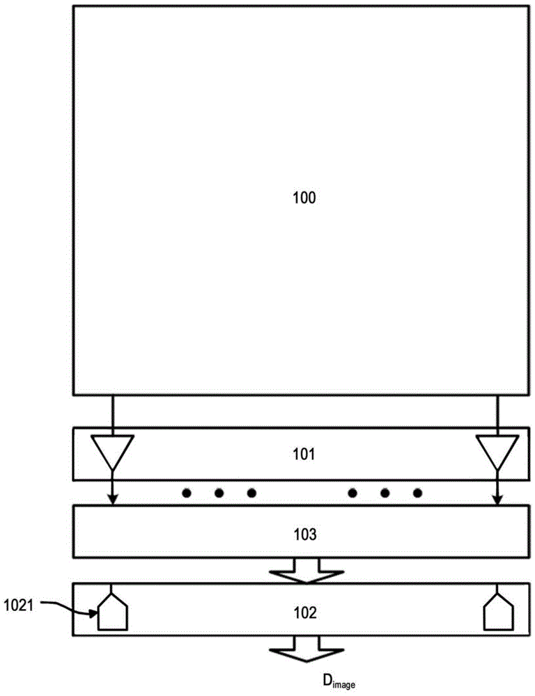
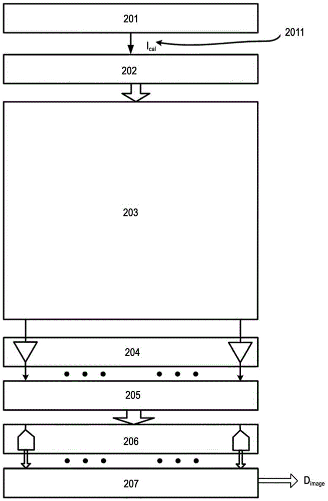
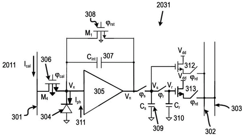
[0040] The present invention aims at the problem that the integration capacitance in the CMOS image sensor in the prior art is relatively large so that the sensitivity is low, and proposes to use the small parasitic coupling formed between the ...


PUM


Abstract

The invention provides a CMOS active pixel image sensor and a calibrating method thereof. The CMOS active pixel image sensor comprises a pixel array formed by a plurality of CMOS active pixels. Each pixel comprises a photosensor generating photocurrent under irradiation of incident light, an amplifier the input end of which is coupled with the photosensor, the amplifier being used for amplifying the photocurrent generated by the photosensor, and an integrating capacitor which is coupled between the input end and the output end of the amplifer and used for integration of the photocurrent amplified by the amplifier and for acquisition of integrating voltage, wherein the integrating capacitor is formed via parasitic coupling between metal layers or polycrystalline silicon layers formed in the manufacturing process of the CMOS active pixel image sensor. According to the invention, the integrating capacitor with low capacitance is formed via parasitic coupling between metal layers or polycrystalline silicon layers formed in the manufacturing process of the CMOS active pixel image sensor, so that the sensitivity of the CMOS active pixel image sensor is remarkably increased.

Description

technical field [0001] The invention relates to the field of image sensors, in particular to a CMOS active pixel image sensor and a calibration method thereof. Background technique [0002] Complementary metal oxide semiconductor (CMOS) image sensor (CIS) has become the mainstream of imaging technology due to its small size, low power consumption and low cost, and is widely used in optical mice, digital cameras, videophones, Smartphones and more. [0003] For CMOS image sensors, sensitivity and noise are two important parameters that usually measure the level of a digital image sensor, and since the fixed pattern noise (FPN) in the noise is constant for each frame, it is a bit like passing through the grid Looking at things, so fixed pattern noise reduction is more valued than transient noise reduction. [0004] The existing CIS technology is a CMOS image sensor composed of a pixel array (pixel array), and the pixel array is formed by arranging many pixel units. The genera...

Claims


Application Information

Patent Timeline
Patent Type & Authority Patents(China)
IPC IPC(8): H04N5/374H04N5/3745H01L27/146
Inventor 袁杰徐若愚
Owner THE HONG KONG UNIV OF SCI & TECH
Why Eureka
Try Eureka