Semiconductor storing device and semiconductor integrated circuit

A storage device and semiconductor technology, applied in semiconductor devices, semiconductor/solid-state device manufacturing, static memory, etc., can solve problems such as prolonging the time required for data readout, difficulty in identifying cell current or leakage current, and misreading data.

Inactive Publication Date: 2005-11-02
PANASONIC CORP
View PDF0 Cites 0 Cited by
  • Summary
  • Abstract
  • Description
  • Claims
  • Application Information

AI Technical Summary

Problems solved by technology

The above-mentioned existing negative voltage word line driving technology, etc., will further induce the problem of GIDL leakage current, and there is a problem that such a new leakage current cannot be suppressed
[0006] In particular, regarding the leakage current from the bit line, in the output read operation, in determining whether or not the potential of the precharged bit line is drawn from the cell current, when there is a non-negligible amount of leakage current on the bit line relative to the cell current When there is a leakage current, it is difficult to identify whether it is the cell current or the leakage current, which will either prolong the time required for data readout, or cause the problem of misreading data

Method used


Image

  • Semiconductor storing device and semiconductor integrated circuit
  • Semiconductor storing device and semiconductor integrated circuit
  • Semiconductor storing device and semiconductor integrated circuit

Examples


no. 1 Embodiment

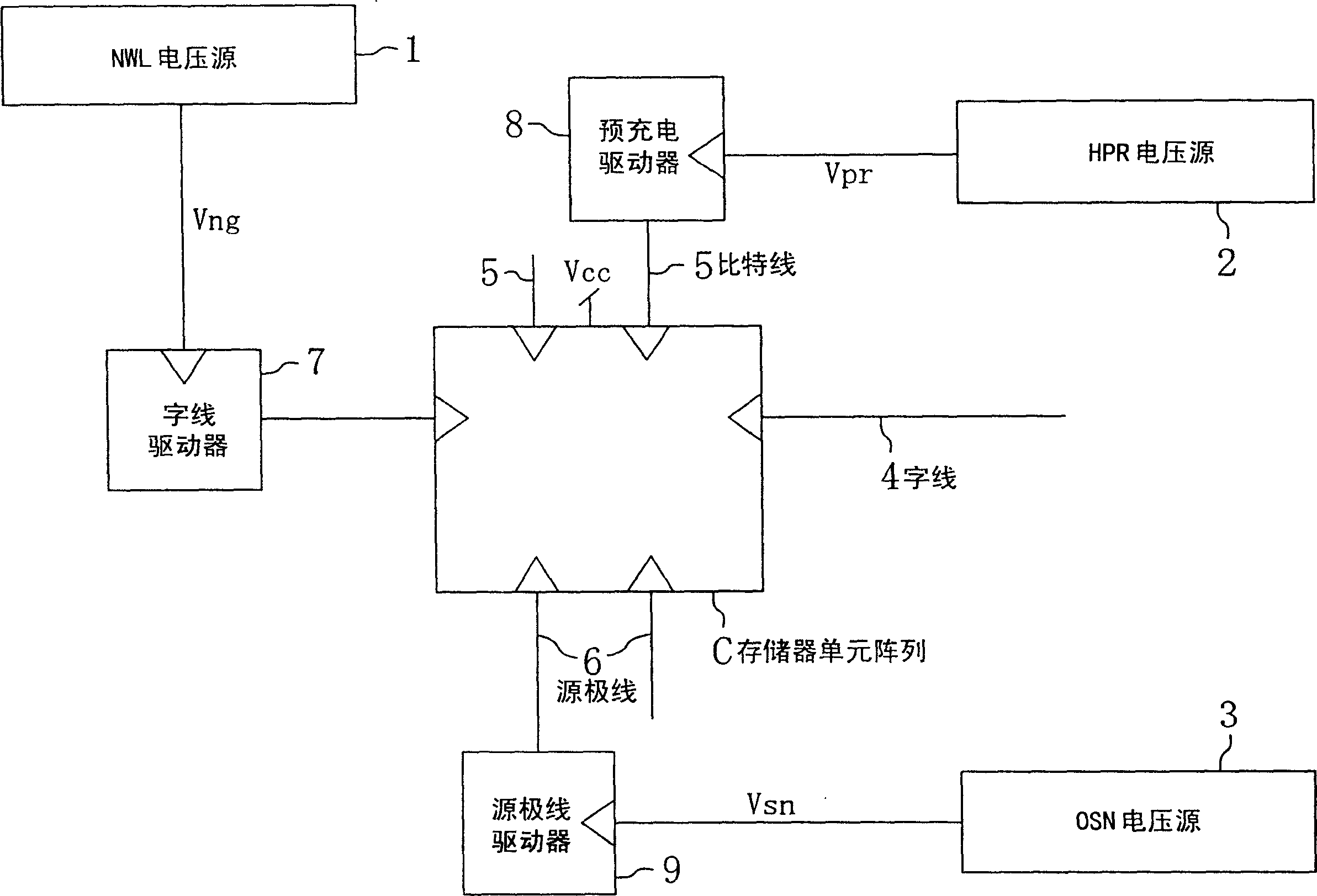
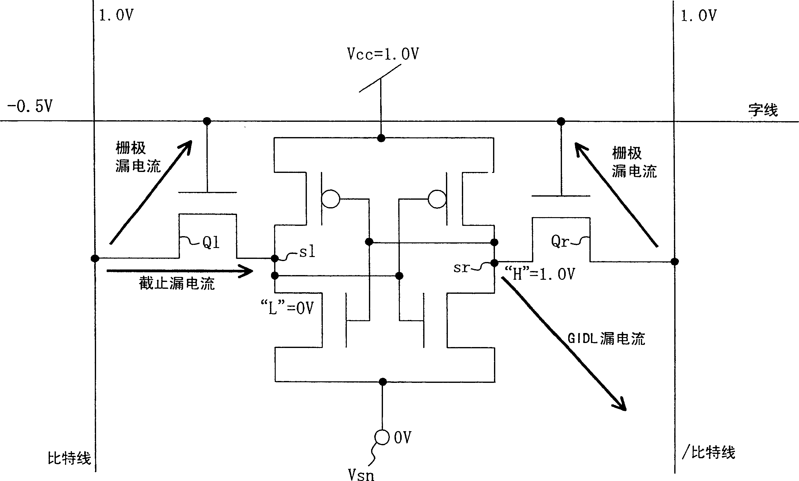
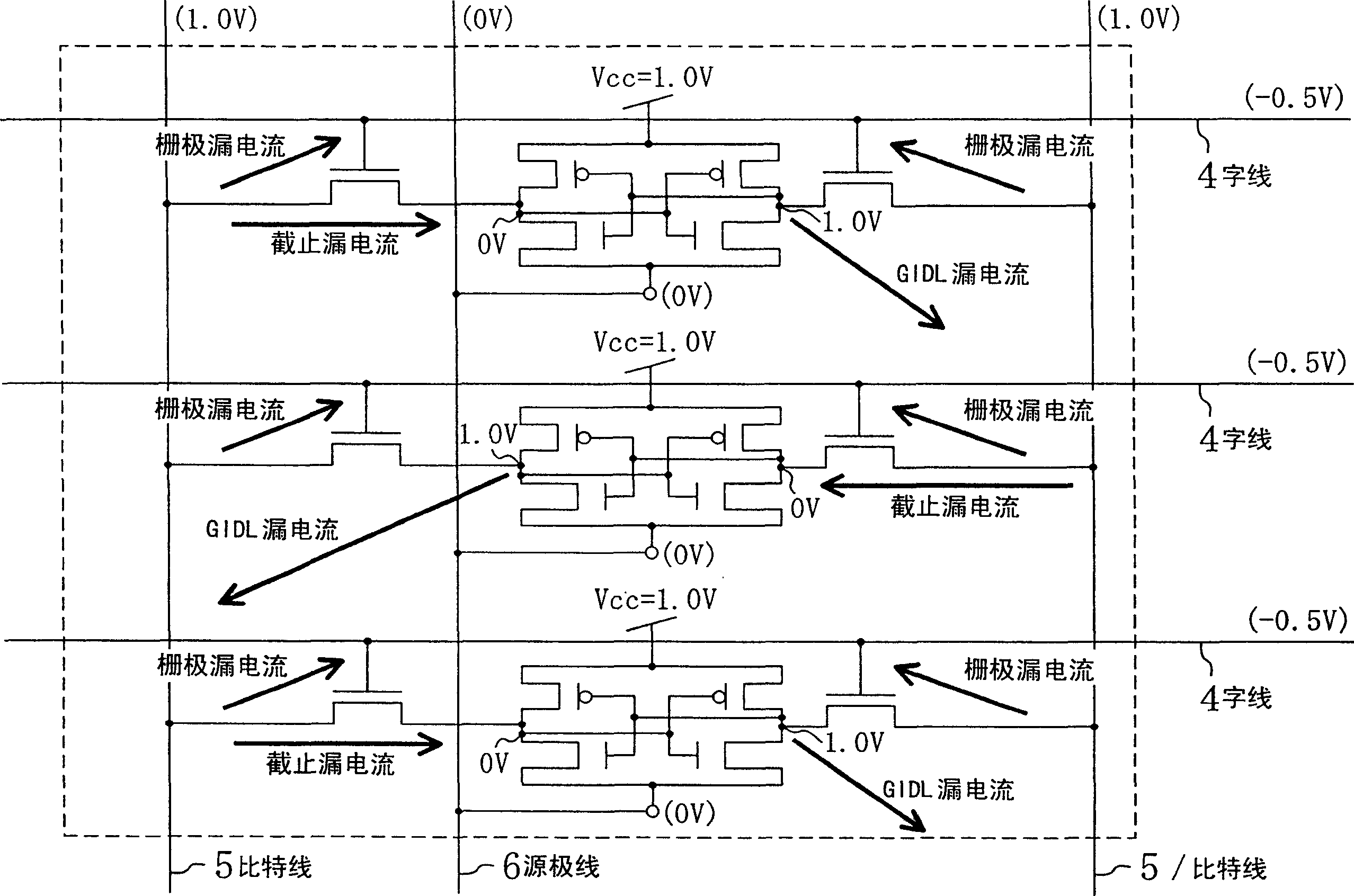
[0053] figure 1 A SRAM as a semiconductor memory device according to a first embodiment of the present invention is shown. In this figure, C represents the memory cell array, such as figure 2 As shown, two NMOS transistors and two PMOS transistors constituted by connecting two inverter circuits to form flip-flops, and two access transistors Ql and Qr arranged on the left and right are included as one memory cell. A plurality of memory cells are arranged in the column direction and the column direction. The two access transistors Ql and Qr constituting the memory cell have a large gate leakage current, and the difference between the off leakage current and the gate leakage current per unit gate width at normal temperature is within 2 digits. It is effective to apply the present invention when transistors Q1 and Qr having this characteristic are used.

[0054] In addition, in figure 1 as well as figure 2 Among them, 5 and 5 denote two paired bit lines connected to the sto...

no. 2 Embodiment

[0073] Then, refer to Figure 10 A semiconductor integrated circuit according to a second embodiment of the present invention will be described. This embodiment relates to the internal structure of the word line driver in the SRAM described in the first embodiment.

[0074] exist Figure 10 Among them, 15 represents SRAM, and inside it, although not shown in the figure, it has the above-mentioned figure 2 A plurality of memory cells and bit lines that have been described in , and a plurality of word lines 4 (only one is shown in this figure). Further, in the SARM 15, a decoder (decoding circuit) 16 for selecting any one of the plurality of word lines and a word line driver (word line driver circuit) for driving the selected word line 4 after receiving the output of the decoder 16 are included. 17. The above-mentioned SARM 15 may also be constituted by the SRAM described in the above-mentioned first embodiment.

[0075] In this figure, 20 denotes a first logic circuit, 21...

no. 3 Embodiment

[0092] Finally, a third embodiment of the present invention will be described. In this embodiment, a ROM is used as a semiconductor memory device.

[0093] In a ROM, since the number of memory cells connected to one bit line is relatively large, the influence of gate leakage current of a cell transistor between a non-selected word line and a bit line becomes relatively large. As already explained, if the negative potential of the non-selected word line is made relatively deep (the maximum value is a large value), although the off-leakage current is limited, when the bit line is selectively precharged with the power supply voltage, the bit line- The potential difference between the word lines exceeds the power supply voltage, increasing the gate leakage current. As a result, the potential of the precharged bit line is pulled to the negative potential of a plurality of non-selected word lines instead of the original source line, and greatly drops, causing a malfunction in readi...


PUM


Abstract

In a semiconductor memory device, a precharge potential for non-selected bit lines among a plurality of bit lines, supplied by a HPR voltage source, is set at a value (for example, 1 / 2 Vcc=0.4 V) lower than the power supply voltage Vcc (low voltage in the range of 0.5 V to 1.2 V; for example, 0.8 V) determining the high-level side potential of data stored in a memory cell. A potential for non-selected word lines among a plurality of word lines, supplied by a NWL voltage source, is set at a predetermined negative potential (for example, - 1 / 4 Vcc=-0.2 V). The total of the precharge potential (0.4 V) of non-selected bit lines and the absolute value of the negative potential (-0.2 V) of non-selected word lines is set at a value less than the power supply voltage Vcc (0.8 V). By these settings, gate leakage current and GIDL current can be effectively limited to a small value while realizing effective limitation of OFF leakage current in a plurality of memory cells.

Description

technical field [0001] The present invention relates to a single semiconductor memory device and a semiconductor integrated circuit including the semiconductor memory device, in particular to a high integration and high density with a power supply voltage below 1.2V and a design wire gauge below 0.13 μm for operation at a low voltage A technology that can effectively reduce the leakage current of a transistor when using a device. Background technique [0002] In general, in order to enable a semiconductor memory device to operate at a high speed even at a low voltage, a technique of using a transistor with a low threshold voltage as its constituent transistor is employed. [0003] Under such circumstances, in a low-threshold voltage transistor, a large off-leakage current flows between the source and the drain even when the transistor is off. In order to solve this problem, in the prior art, for example, by setting the word line to a negative voltage or moving the source po...

Claims


Application Information

Patent Timeline
Patent Type & Authority Patents(China)
IPC IPC(8): G11C11/41G11C7/12G11C11/417G11C11/4193H01L21/8244H01L21/8246H01L27/11H01L27/112
CPCG11C7/12G11C11/34
Inventor 山内宽行
Owner PANASONIC CORP
Why Eureka
Try Eureka