Method of manufacturing a structure based on anisotropic etching, and silicon substrate with etching mask

a technology of anisotropic etching and manufacturing method, which is applied in the direction of photomechanical treatment originals, instruments, photomechanical equipment, etc., can solve the problems of reducing the yield of products, affecting the product quality of products, and the base etching mask, so as to reduce the deficient product ratio of the structure

Inactive Publication Date: 2009-06-25
CANON KK
View PDF6 Cites 2 Cited by
  • Summary
  • Abstract
  • Description
  • Claims
  • Application Information

AI Technical Summary

Benefits of technology

[0005]The present invention provides a method of manufacturing a structure based on anisotropic etching by which at least one of the inconveniences described above can be prevented or reduced.
[0017]Since the present invention uses a correction etching mask having a lowered-strength portion as described above, the possibility of peeling off or damaging the correction etching mask, which leads to a base etching mask, is reduced. Hence, the possibility that the final shape of the structure formed by the etching differs from a desired target shape can be reduced, and therefore, the deficient product ratio of the structure can be reduced.

Problems solved by technology

When a target shape is made by using anisotropic wet etching of silicon, there is a possibility that, during the etching process or after the etching process, a correction etching mask, which leads to a base etching mask, may come off or become damaged.
However, if the accuracy in the shape is strictly required in such a portion, this leads to a decreased yield of the products.

Method used


Image

  • Method of manufacturing a structure based on anisotropic etching, and silicon substrate with etching mask
  • Method of manufacturing a structure based on anisotropic etching, and silicon substrate with etching mask
  • Method of manufacturing a structure based on anisotropic etching, and silicon substrate with etching mask

Examples


working examples

[0103]Referring to the drawings, several working examples of the present invention will be explained.

working example 1

[0104]Referring to FIGS. 1A, 1B, 2A, 2B, 3A, and 3B, the structure of an optical deflector, a driving method, and a manufacturing method thereof according to a first working example will be explained.

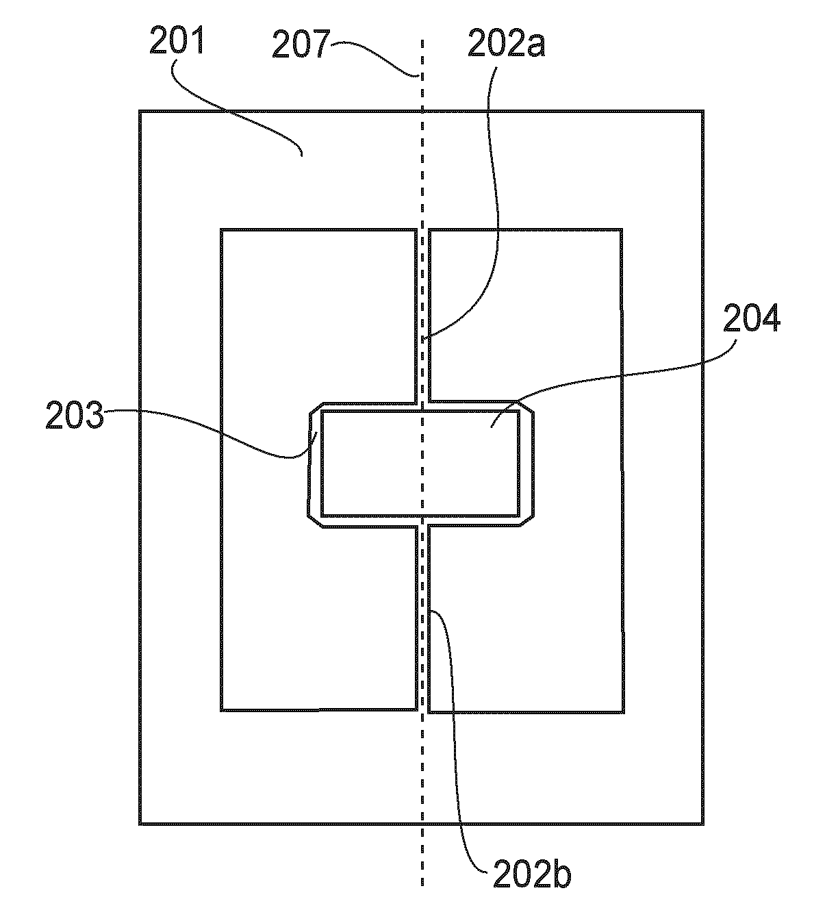
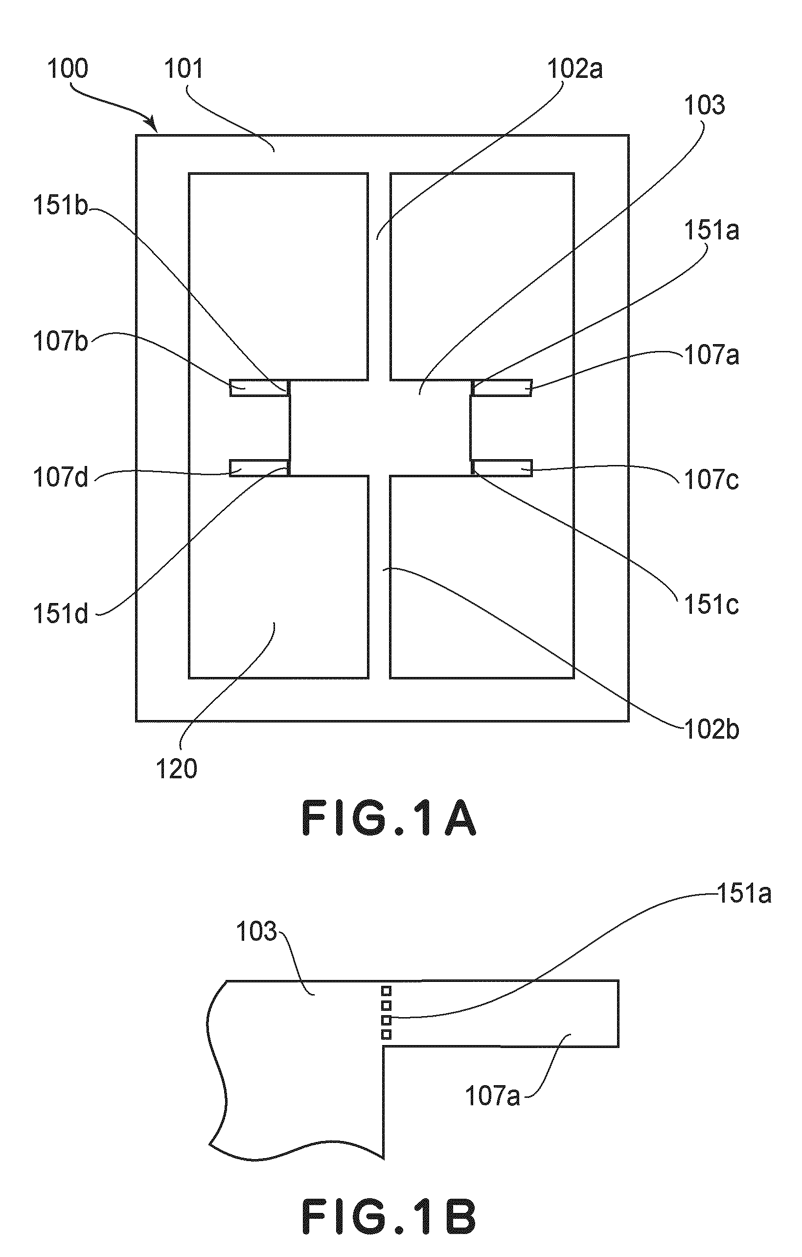
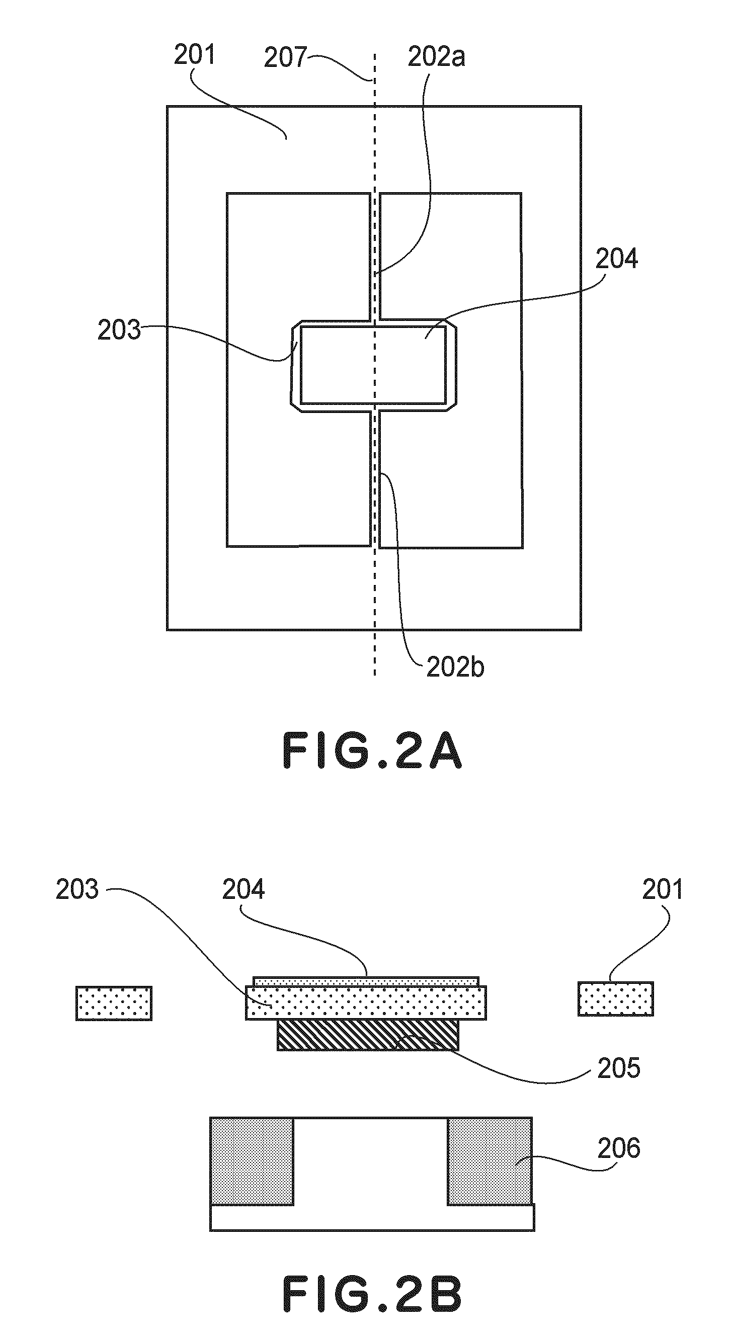
[0105]FIG. 1A is a top plan view of an etching mask of an optical deflector of the present embodiment, and FIG. 1B is an enlarged view of the correction etching mask of FIG. 1A, for explaining the etching mask of the present working example. FIGS. 2A and 2B are diagrams illustrating an optical deflector made by etching a monocrystal silicon substrate by the anisotropic etching.

[0106]As shown in FIGS. 2A and 2B, the optical deflector of this working example comprises a supporting member 201, a movable member 203, and resilient supporting members 202a and 202b. The resilient supporting members 202a and 202b function to resiliently connect the movable member 203 to the supporting member 201 for oscillation around the torsion axis 207. There is a reflection surface 204 formed on the movable...

working example 2

[0113]Referring to FIGS. 8, 2A, 2B, 9A and 9B, a structure manufacturing method of the second working example will be explained. FIG. 8 is a top plan view illustrating the etching mask of the optical deflector of the present working example, and FIGS. 9A and 9B are enlarged views of the correction etching mask of FIG. 8 for explaining an etching mask of the present working example. The structure and the driving method of the optical deflector of the second working example are approximately the same as those of the optical deflector of the first working example.

[0114]In the manufacturing method of the present working example, a silicon nitride film is layered on both surfaces of the monocrystal silicon substrate 700 to a thickness of about 2000 angstroms in accordance with the LPCVD method. Since the silicon nitride film has a high resistance to a potassium hydroxide solution, it is not removed while the silicon substrate 100 is etched by the anisotropic etching solution. Subsequentl...


PUM

PropertyMeasurementUnit
thicknessaaaaaaaaaa
lengthaaaaaaaaaa
lengthaaaaaaaaaa

Abstract

A method of manufacturing a structure that includes a mask forming step for forming, on a monocrystal silicon substrate, a base etching mask corresponding to a target shape and a correction etching mask having a joint connecting to the base etching mask, and a target shape forming step for forming the target shape by anisotropically etching the silicon substrate, wherein, in the mask forming step, a lowered-strength portion where a mechanical strength is locally decreased is formed at least in a portion of the joint of the correction etching mask.

Description

FIELD OF THE INVENTION AND RELATED ART[0001]This invention relates to a method of manufacturing a structure based on anisotropic etching and to a silicon substrate with an etching mask. More particularly, the invention concerns a method of manufacturing a monocrystal silicon substrate with an etching mask and a structure (e.g., microstructure), such as an optical deflector, using the monocrystal silicon substrate, and an optical instrument, such as an optical deflector, manufactured by the manufacturing method. The optical deflectors to be manufactured by this manufacturing method can be suitably used in a projection display device for projecting an image by scanning deflection of light or an image forming apparatus, such as a laser beam printer or a digital copying machine employing an electrophotographic process.[0002]Micromechanical members to be produced from a silicon substrate by a semiconductor process can have a processing precision of a micrometer order. Thus, various micro...

Claims


Application Information

Patent Timeline
Patent Type & Authority Applications(United States)
IPC IPC(8): G02B26/08G03F7/20G03F1/00B81C1/00G02B26/10
CPCB81C1/00404
Inventor NOGUCHI, KAORUHOTTA, YOSHIOTORASHIMA, KAZUTOSHISETOMOTO, YUTAKA
Owner CANON KK
Why Eureka
Try Eureka