Semiconductor device, method of manufacturing the same, and production equipment of the same

Inactive Publication Date: 2009-06-25
GK BRIDGE 1
View PDF5 Cites 3 Cited by
  • Summary
  • Abstract
  • Description
  • Claims
  • Application Information

AI Technical Summary

Benefits of technology

[0015]The present invention has been made to solve such conventional problems, and its object is to lower the profile of a semiconductor device that is a semiconductor laser device wh

Problems solved by technology

More specifically, with the aforementioned conventional semiconductor device, achieving a semiconductor device with a thickness of less than 2.4 mm, and in particular, a semiconductor device with a thickness equal to or less than 2 mm is difficult.
In addition, in the event that lowerin

Method used


Image

  • Semiconductor device, method of manufacturing the same, and production equipment of the same
  • Semiconductor device, method of manufacturing the same, and production equipment of the same
  • Semiconductor device, method of manufacturing the same, and production equipment of the same

Examples


Example

First Embodiment

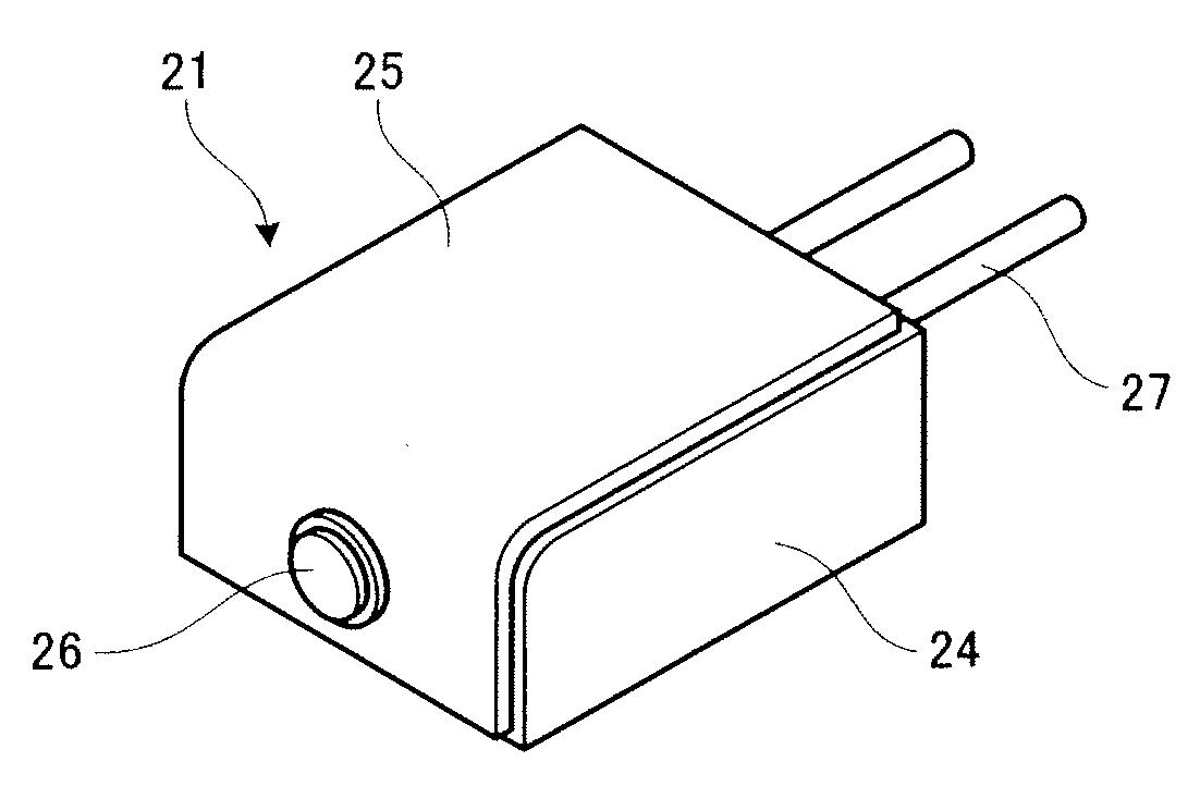
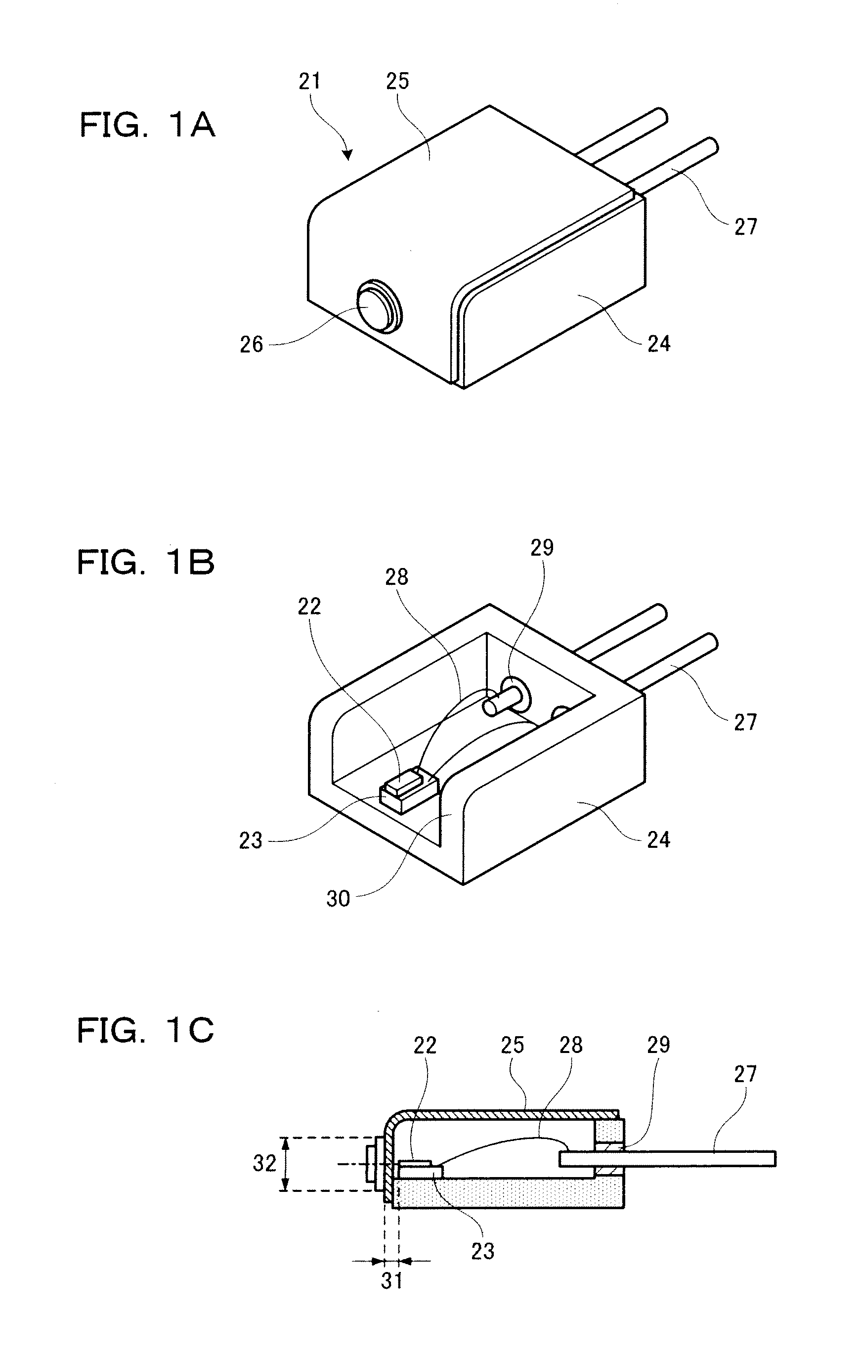
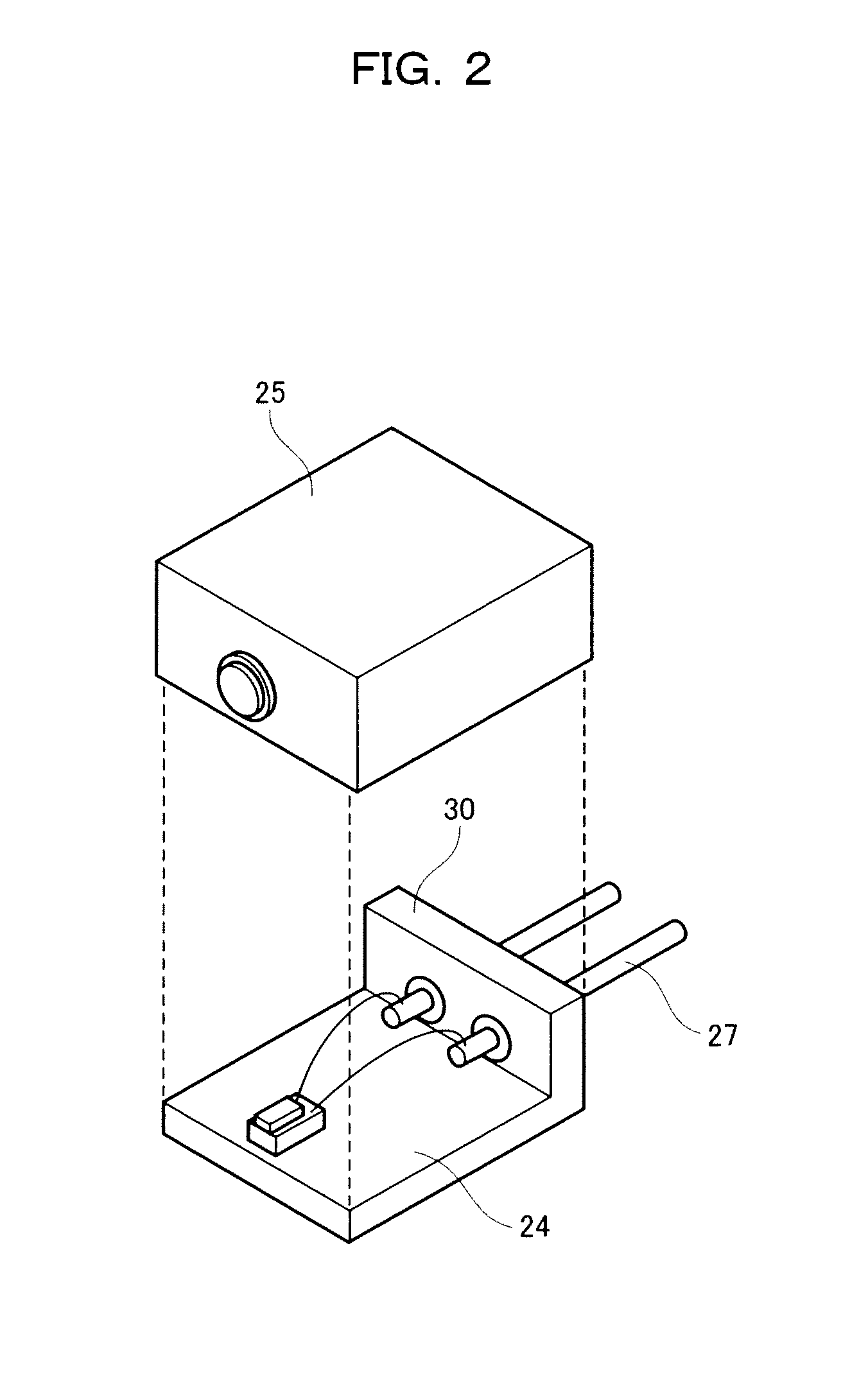
[0051]A first embodiment will now be described using FIGS. 1A, 1B, 1C, 2, 3A, 3B, 4A, 4B, 4C, 5, 6, and 7.

[0052]FIGS. 1A, 1B, and 1C are diagrams showing the configuration of a semiconductor device according to the first embodiment. FIG. 1A is a perspective view; FIG. 1B is a perspective view in which a cap has been removed to offer a better view of an internal configuration of the semiconductor device; and FIG. 1C is a cross-sectional view. FIG. 2 is a diagram showing the configuration of the semiconductor device whose lateral face is formed by a cap, according to the first embodiment. FIGS. 3A and 3B are diagrams showing the configuration of the semiconductor device whose aperture face is formed by an inclined cap, according to the first embodiment. FIG. 3A is a perspective view; and FIG. 3B is a perspective view in which the cap has been removed to offer a better view of an internal configuration of the semiconductor device. FIGS. 4A, 4B, and 4C are diagrams showi...

Example

Second Embodiment

[0071]FIGS. 8A, 8B, 8C, and 8D are diagrams describing a method of manufacturing a semiconductor device according to a second embodiment. FIG. 8A is a perspective view showing a situation where sides on both sides of a frame body of a package and an upper face of the package are welded, and production equipment; FIG. 8B is a schematic diagram showing the situation where the sides on both sides of the package frame body and the upper face of the package are welded, and the production equipment; FIG. 8C is a cross-sectional view showing the situation where the sides on both sides of the package frame body and the upper face of the package are welded; and FIG. 8D is a perspective view showing a situation where a base of an aperture face of the package and the upper face are welded.

[0072]In FIGS. 8A, 8B, 8C, and 8D, the production equipment of a semiconductor device according to the present invention includes: a mechanism (not shown) for conveying and fixing a semicondu...

Example

Third Embodiment

[0076]FIG. 9 is a schematic diagram showing an optical pickup device according to a third embodiment. The schematic diagram shows an optical pickup device 101 mounted with the semiconductor device presented in the first embodiment.

[0077]In FIG. 9, laser light 102 outputted from a semiconductor laser chip (not shown) of a semiconductor device 100 is collimated to parallel light by an optical component 103 such as a collimating lens, has its optical path bent by 90 degrees by an erecting mirror 104, and is focused on a pit recorded on an optical disk 106 by an objective lens 105. Having read a signal on the pit, the laser light 102 is reflected by the optical disk 106, proceeds along the same route in the opposite direction, and returns to the semiconductor device 100. At this point, the laser light 102 is bifurcated by a diffraction optical component 108 disposed between the optical component 103 and the erecting mirror 104, collected by the optical component 103, and...


PUM


Abstract

A cap 25 having a piece of glass 26 formed at a laser irradiating position and covering a laser irradiating direction and an upper face of a package 24, is mounted onto the package 24 having lateral faces of a frame body 30 formed in three directions other than the laser irradiating direction, so as to reduce the distance between a semiconductor element 22 and the piece of glass and to reduce a radius 32 of the piece of glass 26. The profile of the semiconductor device can be therefore lowered while maintaining the characteristics of a semiconductor laser. In addition, by mounting the semiconductor device, the profile of an optical pickup device can also be lowered.

Description

FIELD OF THE INVENTION[0001]The present invention relates to a semiconductor device that integrates a laser and a light receiving element to be used in a rewritable optical disk, a method of manufacturing the same, and production equipment of the same.BACKGROUND OF THE INVENTION[0002]In recent years, large-capacity rewritable optical disks have rapidly become popular through incorporation into DVD recorders, personal computers, and Blu-ray recorders. Moreover, in the case of optical disks mounted in mobile devices such as a lap-top computer, there have been strong demands for optical disk drives with lower profiles.[0003]In order to lower the profile of an optical disk drive, it is important to lower the profile of an optical pickup device. It is anticipated that such profile-lowering can be achieved in the optical design or the mechanism design of an optical pickup device by revising the structures of primary components while retaining performance and functions of such primary comp...

Claims


Application Information

Patent Timeline
IPC IPC(8): H01S5/022
CPCG11B7/123H01S5/32341H01S5/02216H01S5/02208H01L2224/48091
Inventor HAYAMI, ISAOTATEYANAGI, MASAYA
Owner GK BRIDGE 1
Why Eureka
Try Eureka