Thin multi-chip flex module

a multi-chip, flexible technology, applied in the direction of printed circuit manufacturing, printed circuit components, stacked and attached pcbs, etc., can solve the problems of premature failure, ineffective circulation of air as cooling fluid, and considerable heat generation during operation, so as to achieve cost saving, cost saving, and efficient thermal communication

Inactive Publication Date: 2009-07-02
MICROELECTRONICS ASSEMBLY TECH
View PDF33 Cites 23 Cited by
  • Summary
  • Abstract
  • Description
  • Claims
  • Application Information

AI Technical Summary

Benefits of technology

[0019]It will be appreciated that the most effective module solution may not necessarily be the best in any one particular performance attribute, but rather offers the best overall solution at a given density and DRAM clock speed. Objects of the present invention include at least the following: providing effective solutions for thickness reduction in electronic modules; providing electronic modules that are thinner and more cost effective; providing electronic modules suitable for placement at higher densities; providing improved memory modules for computing applications; providing improved memory modules for blade servers; and, providing a method for manufacturing electronic modules that is cost effective and allows for rework.
[0020]Additional objects of the invention include providing a means for efficient thermal communication between the enclosed integrated circuit devices and the exterior surfaces of the thermally conductive shell in an electronic module; maintaining the shortest thermal path from the surfaces of the enclosed chips to the ambient air outside an electronic module; adapting a portion of an interconnecting thin flexible circuit or thin printed circuit board to provide exterior contact pads for electrical and mechanical mating with existing DIMM type sockets; adapting electronic modules with stackable connections whereby modules may be stacked in vertical and / or lateral configurations; and, providing an improved means for locating passive components in circuit modules. These and other objects and advantages will become apparent from reading the specification in conjunction with the accompanying drawings, which are not necessarily drawn to scale.
[0021]In accordance with one aspect of the invention, a flexible circuit comprises a first flexible dielectric sheet having a conductive pattern on at least one surface thereof; a second flexible dielectric sheet having a conductive pattern on at least one surface thereof; at least one microelectronic device operably coupled to the conductive pattern on at least one of the first and second dielectric sheets; a bond layer joining a portion of the surface areas of the first and second dielectric sheets, wherein a portion of the first and second dielectric sheets are not bonded together; and, a plurality of electrical contacts on the portions of the first and second dielectric sheets that are not bonded together.
[0022]In accordance with another aspect of the invention, a flexible circuit comprises a first flexible dielectric sheet having conductive patterns on both surfaces thereof; a second flexible dielectric sheet having conductive patterns on both surfaces thereof; a plurality of microelectronic devices operably coupled to the conductive patterns on at least one side of each of the first and second dielectric sheets; a bond layer joining a portion of the surface areas of the first and second dielectric sheets, wherein a portion of the first and second dielectric sheets are not bonded together; and, a plurality of electrical contacts on the portions of the first and second dielectric sheets that are not bonded together.

Problems solved by technology

Servers contain, among other electronic components, microprocessors and memory modules, which generate considerable heat during operation.
When multiple memory modules are tightly spaced together inside the tightly packed server chassis, the circulation of air as a cooling fluid becomes ineffective.
Air can be restricted, leading to overheating of memory modules which in turn leads to premature failures including device failures and corrupt data streams.
These characteristics are inter-related and the optimization of one may adversely impact the other; so, a balance must be found among these various characteristics to determine the most effective solution.
However, stacking of chips is accompanied by an increase in cost of the stacked chips.
Also, stacking of chips is accompanied by greater heat that is concentrated between the stacked chips and is more difficult to dissipate which leads to an overall hotter module.
However, the addition of larger heat sinks and heat spreaders is accompanied by an increase in thickness.
In turn, increasing thickness leads to a pressure drop between adjacent modules which impedes the flow of air and adversely affects cooling.
However, flexible circuits can be more expensive than standard PCB based on FR4 materials.
Furthermore, thickness reduction causes a mismatch between the thin laminate or the flexible substrate and the standard connector.
However, when the chips are in an optimal heat path configuration, they may not be in an optimal electrical path configuration.
Usually this results in an increase in the layer count of rigid PWB circuit boards.
This may increase the cost of these special PCBs.
Although the use of flexible circuits in packaging semiconductors and consumer electronics is well known and offers the capability of high density interconnect signal stability at high frequencies, and flexible form factor (connecting sites that are not aligned), the technology based on flexile circuits is not without disadvantages.
Flexible circuits present an overall cost disadvantage, they are inherently a non-rigid form factor and need structural members to be incorporated.
One of the challenges caused by the use of flexible circuits is that it reduces the thickness of the substrate to the point that it becomes incompatible with current standard connectors.
However, solving the thickness issues create other issues.
These thin laminates can reduce thickness of the PCB but may not be good for high density modules and high frequency operations due to the limited number of layers they utilize and their dielectric properties.

Method used


Image

  • Thin multi-chip flex module
  • Thin multi-chip flex module
  • Thin multi-chip flex module

Examples


Embodiment Construction

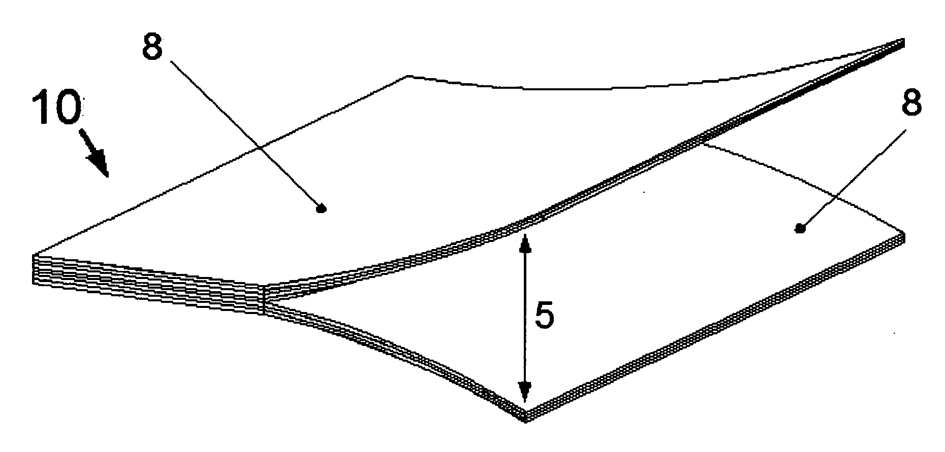
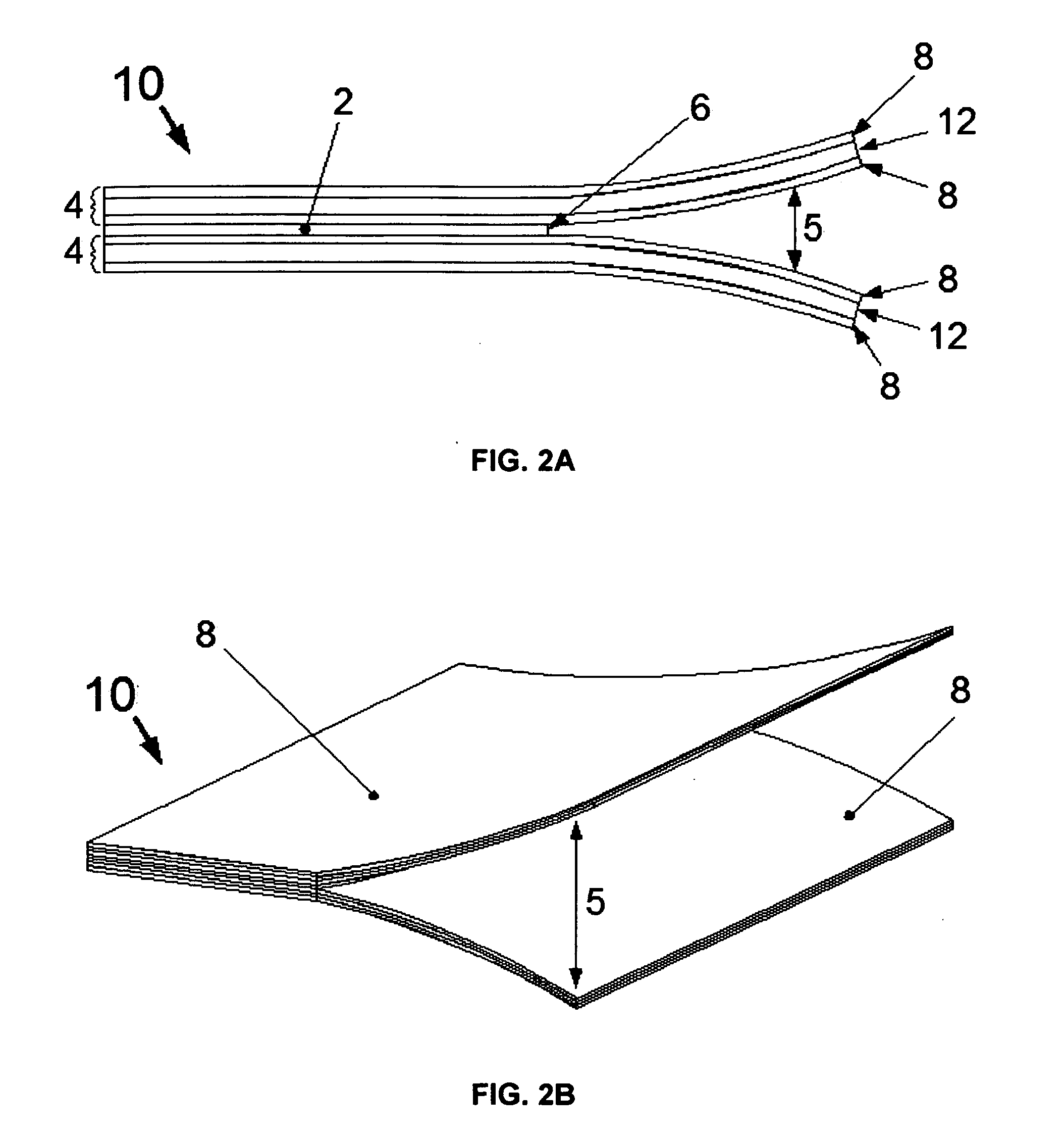
[0053]The present invention addresses the designs of effective solutions to optimize the offering and differentiation for thickness reduction, module densities and relative cost effectiveness. These parameters are balanced per density requirement. For instance, a design that can meet and optimize the attributes of a memory module at the low densities (2 GB and 4 GB) can use a central flexible circuit that places the chips in a mirror image configuration and that offers the benefit of using a lesser amount of flexible circuit and hence enables lower cost. Chips in a mirror image around a flex enable simpler electrical design. Furthermore, the centrally-located flex reduces thickness and when coupled with other features in the current invention (including those features dealing with signal length symmetry, grounding strategies, and the connection interface), would produce an extremely thin and relatively cost effective solution at the low densities.

[0054]Skilled artisans will apprecia...


PUM

PropertyMeasurementUnit
thicknessaaaaaaaaaa
thicknessaaaaaaaaaa
thicknessaaaaaaaaaa

Abstract

A flexible circuit comprises two flexible dielectric sheets having conductive patterns on their surface(s) to which microelectronic device(s) are attached. A bond layer joins the two sheets over a portion of their respective surface areas so that a remaining portion of their areas remain unbonded and a bifurcated structure is thereby formed. Electrical contacts are provided on the unbonded or bifurcated portions of the flexible sheets. The flex may be attached to a rigid frame and provided with protective heat spreading covers.

Description

CROSS-REFERENCE TO RELATED APPLICATION[0001]This application claims the benefit of Provisional Patent Application No. 61 / 009,781 by the present inventors, filed on Jan. 2, 2008, the entire disclosure of which is incorporated herein by reference.BACKGROUND OF THE INVENTION[0002]1. Field of the Invention[0003]The present invention relates generally to means for packaging microelectronic devices and multichip modules. More particularly, the invention relates to improved flex-circuit solutions for SIMM and DIMM type memory modules and other modular electronic circuits.[0004]2. Description of Related Art[0005]High density computing is continually evolving to offer high performance devices with higher densities and smaller form factors. Servers are designed with these goals in mind and are key enablers for various computing applications. Servers contain, among other electronic components, microprocessors and memory modules, which generate considerable heat during operation. Currently high...

Claims


Application Information

Patent Timeline
Patent Type & Authority Applications(United States)
IPC IPC(8): H05K1/00
CPCH05K1/147Y10T29/49144H05K3/0061H05K2201/043H05K2201/056H05K2201/09109H05K2201/10159H05K2201/1056H01L2224/16225H01L2224/73253H01L2924/15311H01L2924/07811H05K1/189Y10T29/49179Y10T29/49124Y10T29/4913H01L2924/00
Inventor CLAYTON, JAMES E.FATHI, ZAKARYAE
Owner MICROELECTRONICS ASSEMBLY TECH
Why Eureka
Try Eureka