Circuit and method for controlling local data line in semiconductor memory device

Inactive Publication Date: 2009-07-02
SK HYNIX INC
View PDF3 Cites 0 Cited by
  • Summary
  • Abstract
  • Description
  • Claims
  • Application Information

AI Technical Summary

Benefits of technology

[0017]Embodiments of the present invention are directed to providing a circuit and method for controlling local data lines in a semico

Problems solved by technology

This structure causes unnecessarily excessive loading on data closer to the input

Method used


Image

  • Circuit and method for controlling local data line in semiconductor memory device
  • Circuit and method for controlling local data line in semiconductor memory device
  • Circuit and method for controlling local data line in semiconductor memory device

Examples


Embodiment Construction

[0026]Hereinafter, a circuit and method for controlling local data lines in a semiconductor memory device in accordance with the present invention will be described in detail with reference to the accompanying drawings.

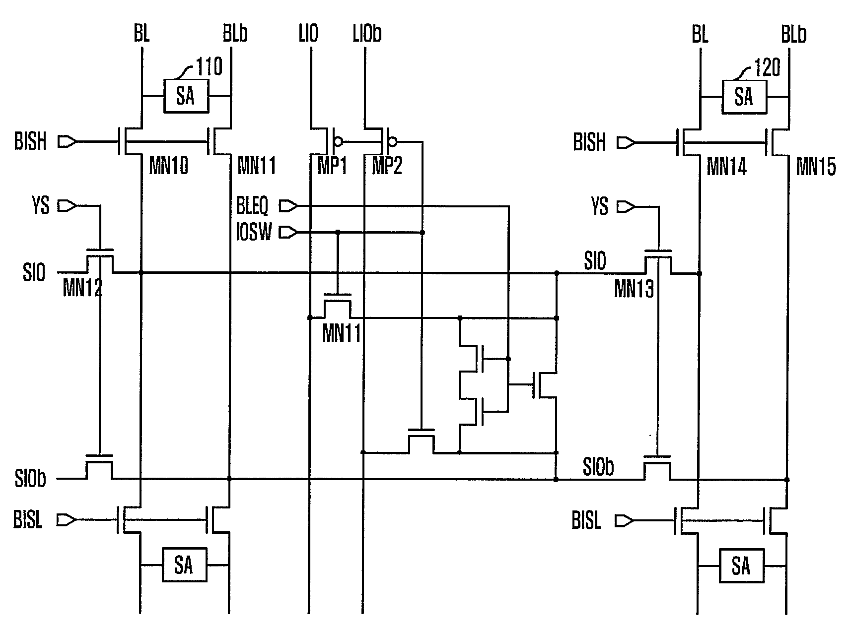
[0027]FIG. 3 schematically shows the arrangement of local data lines in a memory device in accordance with the present invention. FIG. 4 is a circuit diagram for controlling local data lines in accordance with the present invention.

[0028]As shown in FIGS. 3 and 4, local data lines LIO serve to transfer cell data to a bit line BL selected when a transistor MN14 is turned on by bit line selection signals BISH and BISL. The local data lines LIO serve to transfer the data on the bit line to a segment input / output line SIO, when a transistor MN13 is turned on by a control signal YS in response to a read address. Then, when a transistor MN11 is turned on by a line switch control signal IOSW, the data on the SIO is transferred to the connected local data line LIO. The line s...


PUM


Abstract

The present invention relates to a semiconductor memory device, and more particularly, to a circuit and method for controlling local data lines, which can reduce loading on local data lines LIO. The circuit and method for controlling local data lines in accordance with the present invention is characterized by having different line loading of local data lines depending on positions of cell mats. In addition, local data lines between arrays are connected by a switch. Accordingly, the switch is turned on/off by address information about cell mat arrays, thereby preventing unnecessary line loading of local data lines to completely remove unnecessary loading. Moreover, the present invention reduces line loading, thereby improving data processing speed.

Description

CROSS-REFERENCE TO RELATED APPLICATIONS[0001]The present invention claims priority of Korean patent application number 10-2007-0140413, filed on Dec. 28, 2007, which is incorporated by reference in its entirety.BACKGROUND OF THE INVENTION[0002]The present invention relates to a semiconductor memory device, and more particularly, to a circuit and method for controlling local data lines, which can reduce loading on the local data lines.[0003]There is a need for a circuit for data transmission between a global data line GIO and a local data line LIO. The local data line receives an output from a bit line sense amplifier which is provided from the inside of a memory cell region. The global data line is an input / output data line for data transmission between a data input / output pad and the memory cell region. To this end, an input / output sense amplifier IOSA is used to transmit data loaded on the LIO line to the GIO line during a read operation.[0004]In addition, a memory cell array has ...

Claims


Application Information

Patent Timeline
IPC IPC(8): G11C7/00
CPCG11C7/1048G11C2207/002G11C7/18G11C7/10
Inventor CHI, SUNG-SOO
Owner SK HYNIX INC
Why Eureka
Try Eureka