Organic electroluminescence device and organic-electroluminescence-material-containing solution

Inactive Publication Date: 2009-07-09
IDEMITSU KOSAN CO LTD
View PDF13 Cites 24 Cited by
  • Summary
  • Abstract
  • Description
  • Claims
  • Application Information

AI Technical Summary

Benefits of technology

0152]Since the nitrogen-containing heterocyclic derivative represented by the formulae (201) to (203) each has excellent electron injectability, the electron transporting layer containing the nitrogen-containing heterocyclic derivative can contribute to lowering of voltage of the organic EL device.
0153]By enhancing the electron injectability, a sufficient amount of electrons can be injected into the emitting layer. Thus, it is not necessary to block holes by the electron transp

Problems solved by technology

However, although an organic EL device in which CBP is used as the host exhibits much higher luminous efficiency due to phosphorescent emission, the organic EL device has such a short lifetime as to be practically inapplicable.
Thus, it is not successful to simply apply the host material for fluorescent-emitting layer to a host for phosphorescent emission.
However, triplet energy gap Eg(T) of such compounds is approximately 1.9 eV and thus insufficien

Method used


Image

  • Organic electroluminescence device and organic-electroluminescence-material-containing solution
  • Organic electroluminescence device and organic-electroluminescence-material-containing solution
  • Organic electroluminescence device and organic-electroluminescence-material-containing solution

Examples


example 1

[0246]A glass substrate (size: 25 mm×75 mm×1.1 mm thick) having an ITO transparent electrode (manufactured by Geomatec Co., Ltd.) was ultrasonic-cleaned in isopropyl alcohol for five minutes, and then UV / ozone-cleaned for 30 minutes.

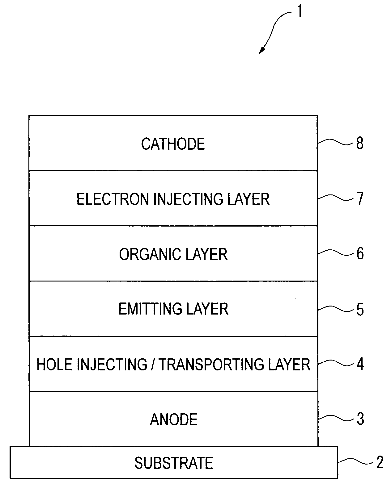
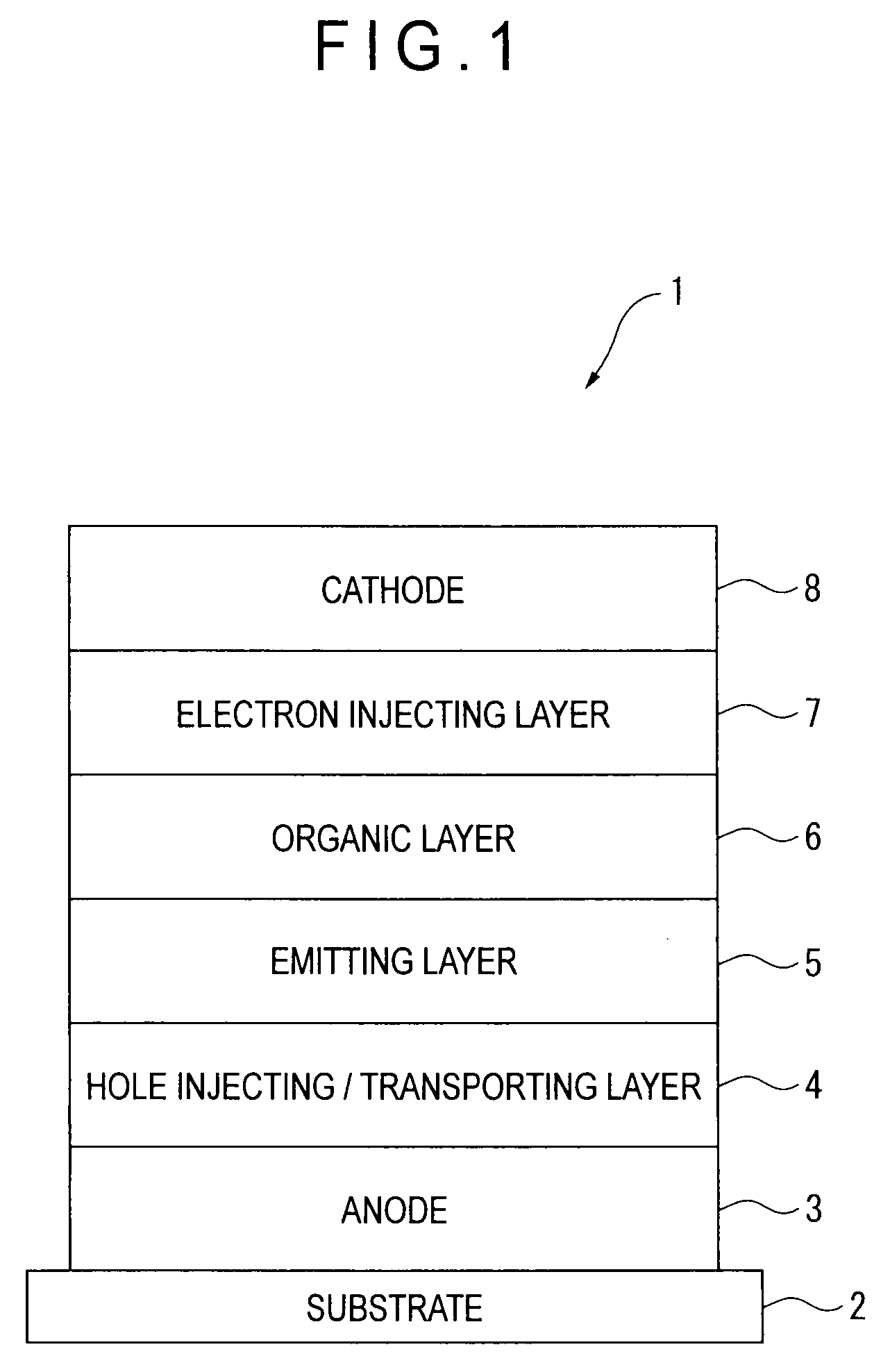
[0247]After the glass substrate having the transparent electrode line was cleaned, the glass substrate was mounted on a substrate holder of a vacuum deposition apparatus. Then, 50-nm thick film of 4,4′-bis[N-(1-naphthyl)-N-phenylamino]biphenyl (hereinafter abbreviated as “NPD film”) was formed initially onto a surface of the glass substrate provided with the transparent electrode line by resistance heating deposition in such a manner that the NPD film covered the transparent electrode. The NPD film served as the hole injecting / transporting layer.

[0248]Then, an emitting layer was formed on the NPD film. The following compound (H1), which was used as the phosphorescent host, was formed into 40-nm thick film by resistance heating deposition. At the same tim...

example 2

[0252]Except that the following compound (H3) was used as the organic layer, the organic EL device according to the Example 2 was manufactured in the same manner as the Example 1.

[Comparative 1]

[0253]Except that Balq (bis-(2-methyl-8-quinolinolate)-4-(phenylphenolate) aluminum) was used as the organic layer, the organic EL device according to the Comparative I was manufactured in the same manner as the Example 1.

[Evaluation of Organic EL Device]

[0254]The organic EL devices each manufactured as described above were driven by direct-current electricity of 1 mA / cm2 to emit light, so that emission chromaticity and voltage were measured. In addition, by conducting a direct-current continuous current test with the initial luminance intensity being set at 5000 cd / m2 for each organic EL device, time elapsed until the initial luminance intensity was reduced to the half (i.e., time until half-life) was measured for each organic EL device.

[0255]The results of the evaluation are shown in Table ...

example 3

[0259]A glass substrate (size: 25 mm×75 mm×1.1 mm thick) having an ITO transparent electrode (manufactured by Geomatec Co., Ltd.) was ultrasonic-cleaned in isopropyl alcohol for five minutes, and then UV / ozone-cleaned for 30 minutes.

[0260]After the glass substrate having the transparent electrode line was cleaned, the glass substrate was mounted on of a substrate holder of a vacuum deposition apparatus. Then, 50-nm thick film of 4,4′-bis[N-(1-naphthyl)-N-phenylamino]biphenyl (hereinafter abbreviated as “NPD film”) was initially formed by resistance heating deposition onto a surface of the glass substrate where the transparent electrode line was provided in a manner of covering the transparent electrode. The NPD film served as the hole injecting / transporting layer.

[0261]Then, an emitting layer was formed on the NPD film. The compound (H1) was formed into 20-nm thick film by resistance heating deposition. At the same time, the compound (D1), which was used as the phosphorescent emitti...


PUM


Abstract

An organic electroluminescence device includes: an anode (3); a cathode (8); and an organic thin-film layer provided between the anode (3) and the cathode (8). The organic thin-film layer includes an emitting layer (5) and an organic layer (6) provided on the emitting layer (5) adjacently to the cathode (8). The emitting layer (5) contains: a first polycyclic fused aromatic compound having a substituted or unsubstituted polycyclic fused aromatic skeleton; and a first phosphorescent material for emitting phosphorescence. The organic layer (6) contains a second polycyclic fused aromatic compound having a substituted or unsubstituted polycyclic fused aromatic skeleton.

Description

BACKGROUND OF THE INVENTION[0001]1. Field of the Invention[0002]The present invention relates to an organic electroluminescence device and an organic-electroluminescent-material-containing solution for forming the organic electroluminescence device.[0003]2. Description of Related Art[0004]An organic electroluminescence device (organic EL device), which includes an organic emitting layer between an anode and a cathode, has been known to emit light using exciton energy generated by a recombination of holes and electrons that have been injected into the emitting layer.[0005]Such an organic EL device, which has the advantages as a self-emitting device, is expected to serve as an emitting device excellent in luminous efficiency, image quality, power consumption and thin design.[0006]Further improvements on an organic EL device include improvements in luminous efficiency. In this respect, in order to enhance internal quantum efficiency, developments on phosphorescent materials that emit l...

Claims


Application Information

Patent Timeline
IPC IPC(8): H01L51/54C09K11/06
CPCC09K11/06C09K2211/1007C09K2211/1011H05B33/20H10K85/626H10K85/6572H10K50/11H10K2101/10
Inventor NISHIMURA, KAZUKIIWAKUMA, TOSHIHIROFUKUOKA, KENICHIHOSOKAWA, CHISHIOKAWAMURA, MASAHIRO
Owner IDEMITSU KOSAN CO LTD
Why Eureka
Try Eureka