Multi-layer package structure and fabrication method thereof

a multi-layer package and fabrication method technology, applied in the direction of electrical apparatus construction details, casings/cabinets/drawers details, semiconductor/solid-state device details, etc., can solve the problems of complex connection methods, low cost efficiency, and inability to achieve the desired level of electrical connection between the conductive material and the signal line, etc., to achieve the structural stability of the multi-layer package structure

Inactive Publication Date: 2009-07-09
WAVENICS +1
View PDF5 Cites 14 Cited by
  • Summary
  • Abstract
  • Description
  • Claims
  • Application Information

AI Technical Summary

Benefits of technology

[0026]According to exemplary embodiments of the present invention, an electric connection method between multiple layers using a metal pin is simpler than the typical electric connection method using a bumper (e.g., a stud or solder) after a metal based material fills via holes. Therefore, a multi-lay...

Problems solved by technology

However, the above connection method often does not give a desired level of electric connection between the conductive material a...

Method used


Image

  • Multi-layer package structure and fabrication method thereof
  • Multi-layer package structure and fabrication method thereof
  • Multi-layer package structure and fabrication method thereof

Examples


Embodiment Construction

[0034]Various embodiments of the present invention will be described in detail with reference to the accompanying drawings.

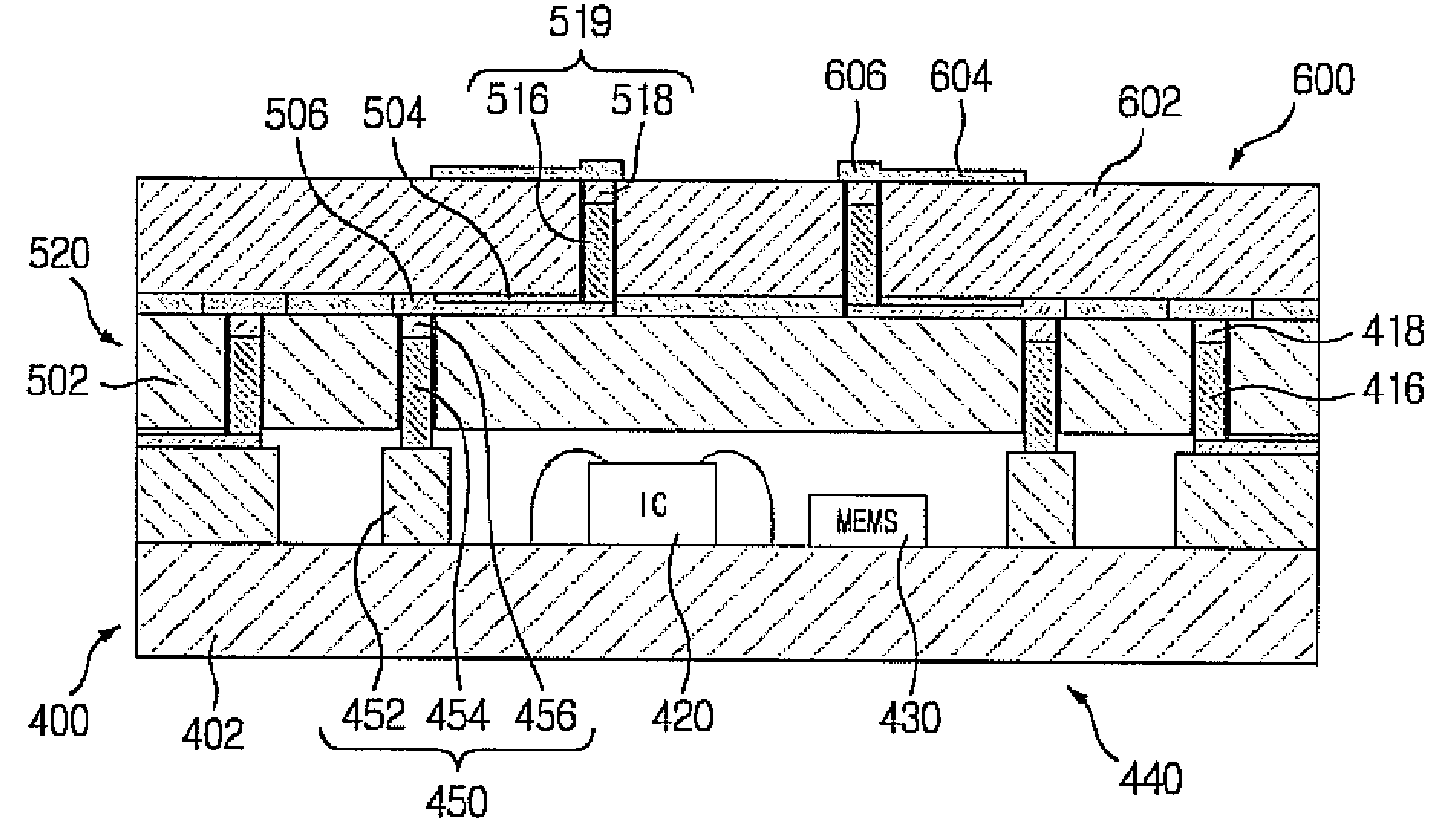
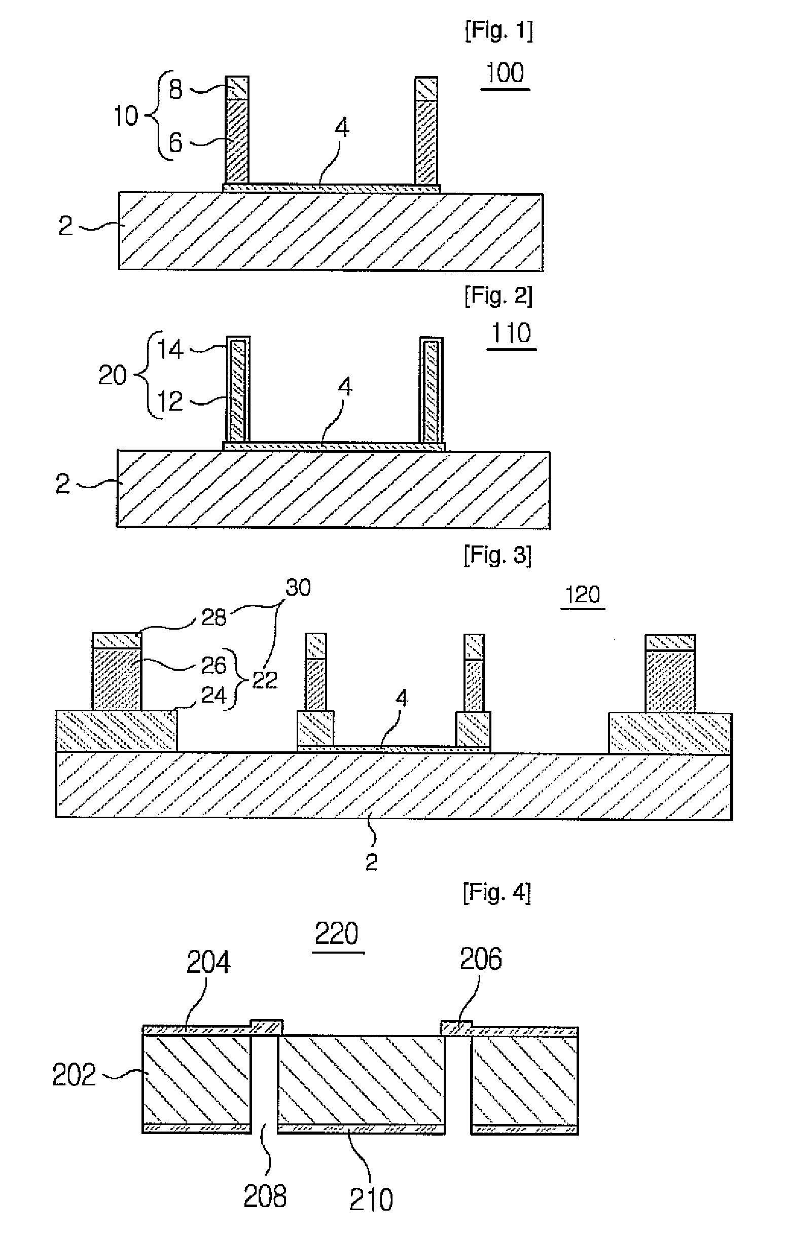
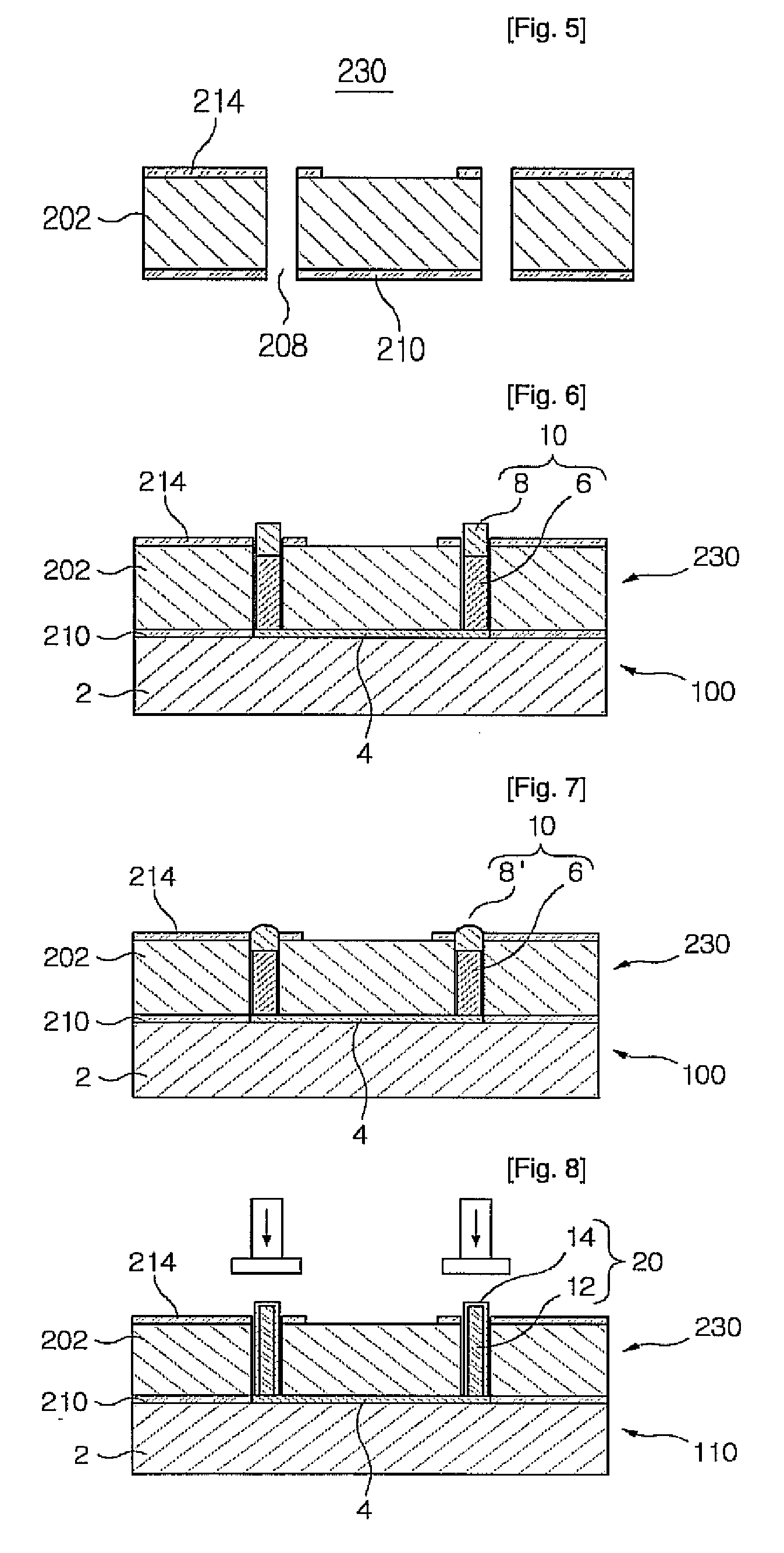
[0035]FIGS. 1 to 3 are cross-sectional views illustrating lower substrate structures with different types of metal pins according to an embodiment of the present invention.

[0036]Referring to FIG. 1, the lower substrate structure 100 includes a base substrate 2 on which an electric signal line 4 (hereinafter referred to as “signal line”) is formed, and metal pins 10 formed over the base substrate 2 and having a high aspect ratio. Each of the metal pins 10 includes a supporting member 6 and a connecting member 8. In more detail of the formation of the metal pins 10, a metal layer is plated on the base substrate 2 on which the electric signal line 4 is formed. Thereafter, a thick photoresist film is coated on the base substrate 2 including the signal line 4 and patterned to expose a plate region. The metal layer of the exposed portion is plated with copper to form ...


PUM

PropertyMeasurementUnit
Timeaaaaaaaaaa
Dielectric polarization enthalpyaaaaaaaaaa
Pressureaaaaaaaaaa

Abstract

A method for allowing an easier electric connection between layers of a multi-layer package structure using a metal pin fabricated based on semiconductor device processes is provided. A metal pin having a high aspect ratio is formed on a lower substrate, while a via hole is formed in an upper substrate. The metal pin is inserted into the via hole and adhered together to make an electric connection between the lower and upper substrates. The metal pin is obtained by patterning a thick photoresist material and plating a material thereon. The metal pin may have a core member obtained by performing a plating process on the surface of a patterned polymer based pin. Solder or gold is used for adhesion and electric connection between the signal line and the metal pin. The above electric connection method can be simpler and have improved structural stability compared with the typical connection method.

Description

TECHNICAL FIELD[0001]The present invention relates to packaging of a semiconductor device, and more particularly, to a multi-layer package structure using a metal pin with a high aspect ratio and a fabrication method thereof.BACKGROUND ART[0002]Among numerous semiconductor device manufacturing processes, packaging is implemented to protect semiconductor chips from external environmental conditions, to form the semiconductor chips in a certain shape to be used conveniently and to protect designed operations of the semiconductor chips. As a result, packaging can improve reliability of a semiconductor device.[0003]As semiconductor devices are becoming highly integrated and being designed to have various functions, packaging is being shifted toward using the increasing number of pins and implementing a surface mounting scheme instead of inserting the package into a printed circuit board (PCB). Many packages implemented with the surface mounting scheme, e.g., a small outline package (SOP...

Claims


Application Information

Patent Timeline
IPC IPC(8): H05K5/02H01R12/00H01R43/00
CPCH01L21/486Y10T29/49213H05K1/0272H05K1/185H05K3/243H05K3/4614H05K3/4638H05K3/4647H05K3/4652H05K3/4679H05K3/4697H05K2201/0394H05K2201/09063H05K2201/09781H05K2203/063H05K2203/0733H05K2203/167H01L2924/0002H01L23/49827B81C1/0023H01L2924/00H05K3/46
Inventor KWON, YOUNG-SEYOOK, JON-MIN
Owner WAVENICS
Why Eureka
Try Eureka