Flip-chip phosphor coating method and devices fabricated utilizing method

a phosphor coating and flip-chip technology, applied in semiconductor/solid-state device manufacturing, semiconductor devices, electrical equipment, etc., can solve the problems of difficult to consistently reproduce leds with the same or similar emission characteristics, difficult to control the geometry and thickness of the phosphor layer, and non-uniform color temperatur

Active Publication Date: 2009-07-16
CREELED INC
View PDF76 Cites 180 Cited by
  • Summary
  • Abstract
  • Description
  • Claims
  • Application Information

AI Technical Summary

Problems solved by technology

Using this method, however, it can be difficult to control the phosphor layer's geometry and thickness.
As a result, light emitting from the LED at different angles can pass through different amounts of conversion material, which can result in an LED with non-uniform color temperature as a function of viewing angle.
Because the geometry and thickness is hard to control, it can also be difficult to consistently reproduce LEDs with the same or similar emission characteristics.
Like the syringe method above, using the stencil method can be difficult to control the geometry and layer thickness of the phosphor containing polymer.
The stenciling composition may not fully fill the stencil opening such that the resulting layer is not uniform.
These problems can result in LEDs having non-uniform color temperature and LEDs that are difficult to consistently reproduce with the same or similar emission characteristics.
One challenge with these approaches is accessing the wire bond pad on the device after the coating process.
Accessing the wire bond by standard wafer fabrication techniques is difficult with typical silicone binding material, as well as other binder materials such as epoxies or glass.
Silicones are not compatible with commonly used wafer fabrication materials such as acetone, as well as some developers, and resist strippers.
This can limit the options and choices for the particular silicones and process steps.
Cured silicone films with phosphor are also difficult to etch and have a very slow etch rate in chlorine and CF4 plasma, and wet etching of cured silicones is typically inefficient.

Method used


Image

  • Flip-chip phosphor coating method and devices fabricated utilizing method
  • Flip-chip phosphor coating method and devices fabricated utilizing method
  • Flip-chip phosphor coating method and devices fabricated utilizing method

Examples


Embodiment Construction

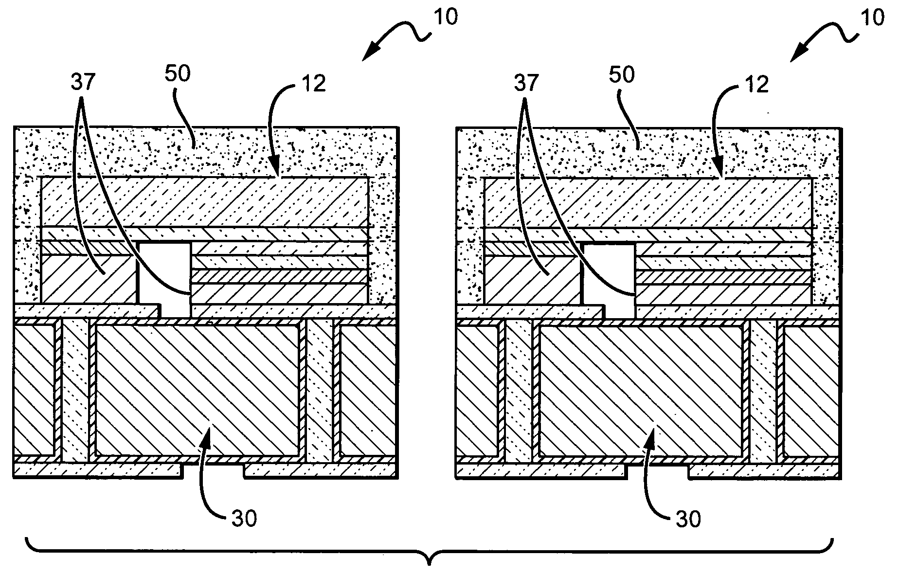
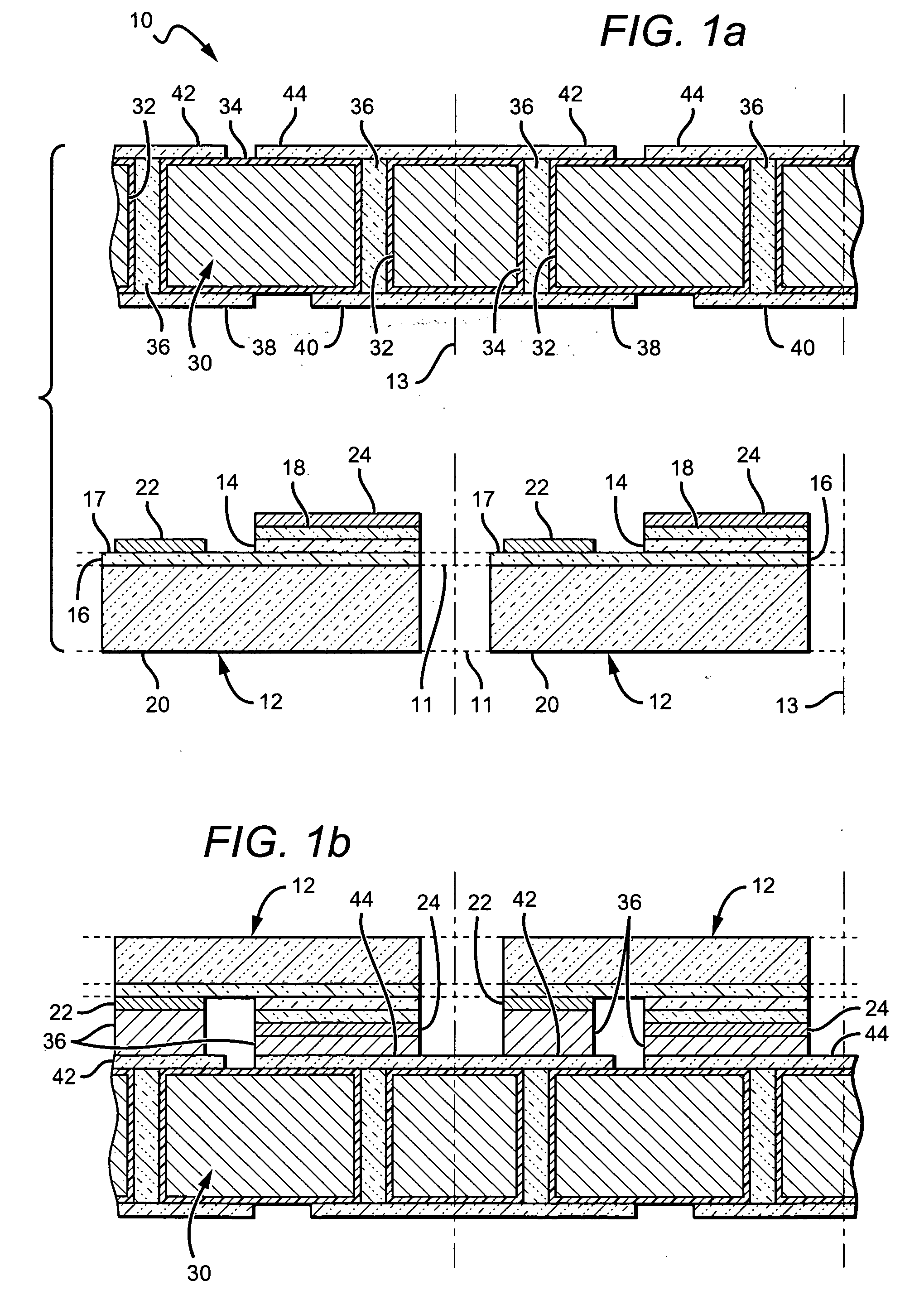
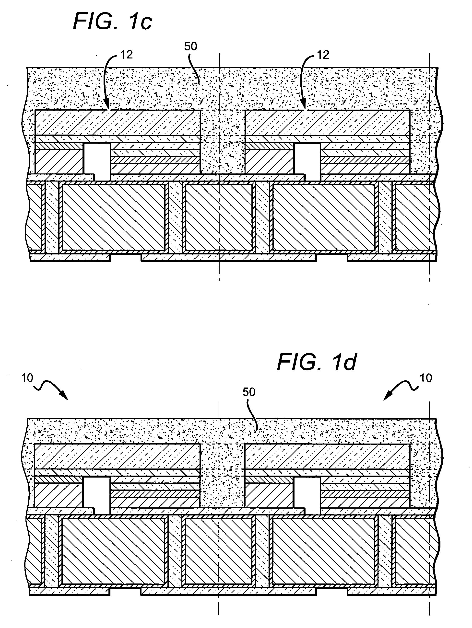
[0034]The present invention provides fabrication methods that are particularly applicable to wafer level coating of semiconductor devices such as LEDs. The present invention also provides semiconductor devices, such as LEDs fabricated using these methods, and related LED packages and LED arrays. In particular the present invention provides for methods of making devices and devices that can be surface mounted and are wire-bond free. A curable blanket coating is provided over the devices that can then be thinned or planarized without the need for gaining electrical access to contacts through the cured material following planarization. Instead, electrical contact is made to the device from the surface opposite the blanket coating. The resulting coating on the top of the devices is continuous and unobstructed by structures such as contacts, bond pads, conductive paths, etc. The coating provides a surface that is particularly adapted for the direct mounting of additional structures, such...


PUM


Abstract

Methods for fabricating light emitting diode (LED) chips one of which comprises flip-chip mounting a plurality of LEDs on a surface of a submount wafer and forming a coating over said LEDs. The coating comprising a conversion material at least partially covering the LEDs. The coating is planarized to the desired thickness with the coating being continuous and unobstructed on the top surface of the LEDs. The LEDs chips are then singulated from the submount wafer. An LED chip comprising a lateral geometry LED having first and second contacts, with the LED flip-chip mounted to a submount by a conductive bonding material. A phosphor loaded binder coats and at least partially covers the LED. The binder provides a substantially continuous and unobstructed coating over the LED. The phosphor within the coating absorbs and converts the wavelength of at least some of the LED light with the coating planarized to achieve the desired emission color point of the LED chip.

Description

BACKGROUND OF THE INVENTION[0001]1. Field of the Invention[0002]This invention relates to methods for fabricating semiconductor devices such as light emitting diodes and light emitting diodes fabricated using the methods.[0003]2. Description of the Related Art[0004]Light emitting diodes (LED or LEDs) are solid state devices that convert electric energy to light, and generally comprise one or more active layers of semiconductor material sandwiched between oppositely doped layers. When a bias is applied across the doped layers, holes and electrons are injected into the active layer where they recombine to generate light. Light is emitted from the active layer and from all surfaces of the LED.[0005]Conventional LEDs cannot generate white light from their active layers. Light from a blue emitting LED has been converted to white light by surrounding the LED with a yellow phosphor, polymer or dye, with a typical phosphor being cerium-doped yttrium aluminum garnet (Ce:YAG). [See Nichia Cor...

Claims


Application Information

Patent Timeline
Patent Type & Authority Applications(United States)
IPC IPC(8): H01L33/00H01L33/44H01L33/50H01L33/64
CPCH01L33/44H01L33/505H01L33/64H01L2933/0041H01L2933/0066H01L33/62H01L27/15H01L33/08H01L33/10H01L33/502H01L2224/13
Inventor CHITNIS, ASHAYIBBETSON, JAMESKELLER, BERND
Owner CREELED INC
Why Eureka
Try Eureka