Junction Structure Between Optical Element and Substrate, Optical Transmission/Receiving Module, and Method of Manufacturing the Optical Module

a technology of optical elements and junction structures, applied in the field of junction structures between optical elements and substrates, optical transmission/receiving modules, and methods of manufacturing optical modules, can solve the problems of increasing light loss, difficult for the under-fill resin to enter the light path, and disadvantageous increase of light loss, so as to improve the efficiency of optical coupling and improve the reliability of physical properties of the junction structure. , the effect of satisfying the junction structur

Inactive Publication Date: 2009-07-16
HITACHI CABLE
View PDF11 Cites 24 Cited by
  • Summary
  • Abstract
  • Description
  • Claims
  • Application Information

AI Technical Summary

Benefits of technology

[0023]With the present invention, it is possible to realize to provide a satisfactory junction structure between an optical element and a substrate with an optical waveguide capable of improving the efficiency in optical coupling and also capable of improving reliability in physical properties of the junction structure by preventing an under-fill or the like containing a filler from entering a light path between the substrate and the optical element, in which the under-fill or the like would otherwise inhibit propagation of outgoing light from the optical element or incoming light into the optical light.

Problems solved by technology

However, in the optical coupling structure described in JP-A-2005-164801, when the resin containing the filler is used as the under-fill resin, because the under-fill resin is provided on the light path, the light loss disadvantageously increases because of light scattering by the filler or for some other reasons.
Therefore, even if the resin containing a filler is used as the under-fill resin, it is difficult for the under-fill resin to enter the light path.
However, because the projection made of a transparent resin is only tightly contacted with the substrate, sometimes the under-fill resin containing a filler enters the space between the projection and the substrate, which may cause increase of light loss.

Method used


Image

  • Junction Structure Between Optical Element and Substrate, Optical Transmission/Receiving Module, and Method of Manufacturing the Optical Module
  • Junction Structure Between Optical Element and Substrate, Optical Transmission/Receiving Module, and Method of Manufacturing the Optical Module
  • Junction Structure Between Optical Element and Substrate, Optical Transmission/Receiving Module, and Method of Manufacturing the Optical Module

Examples


first embodiment

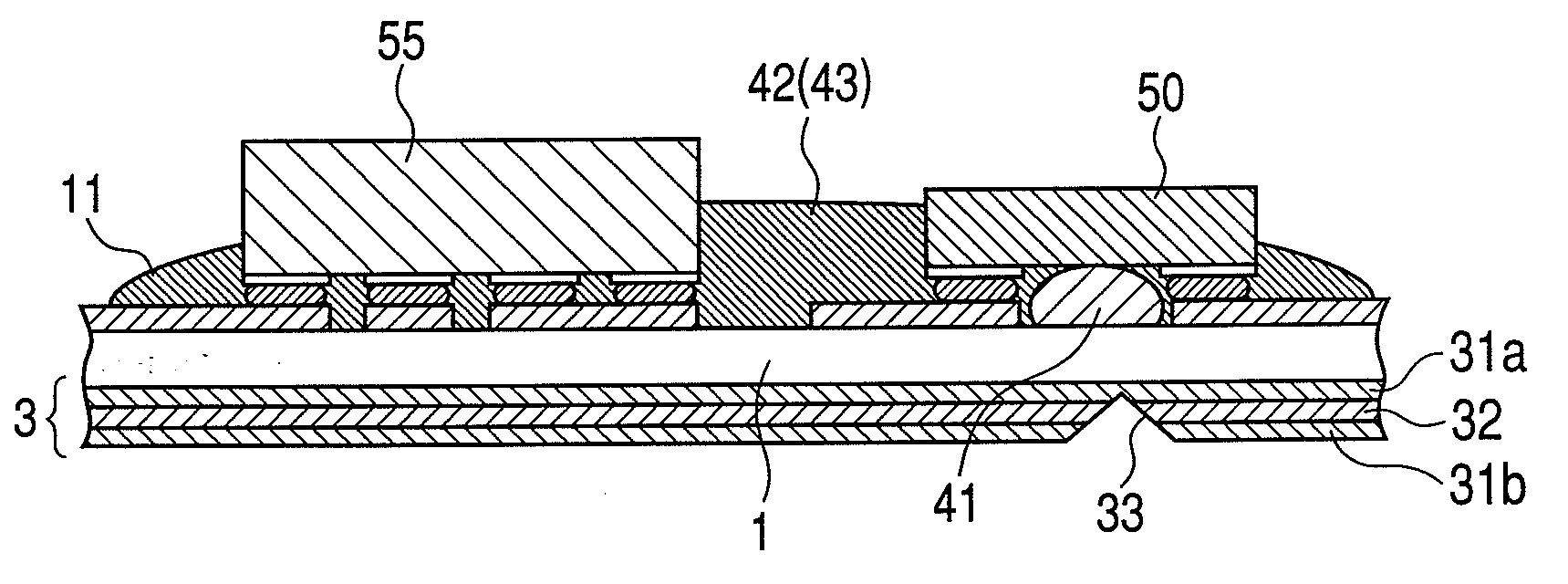
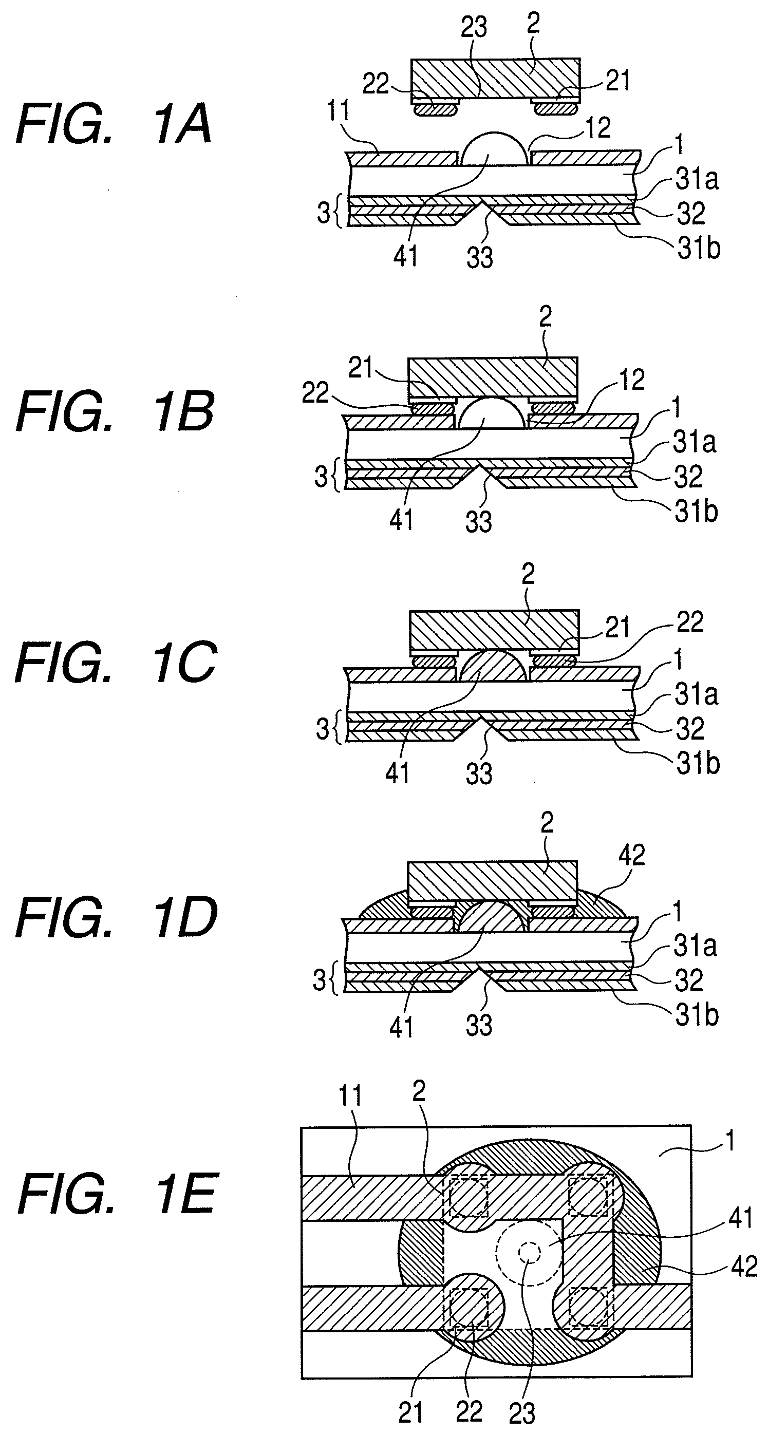
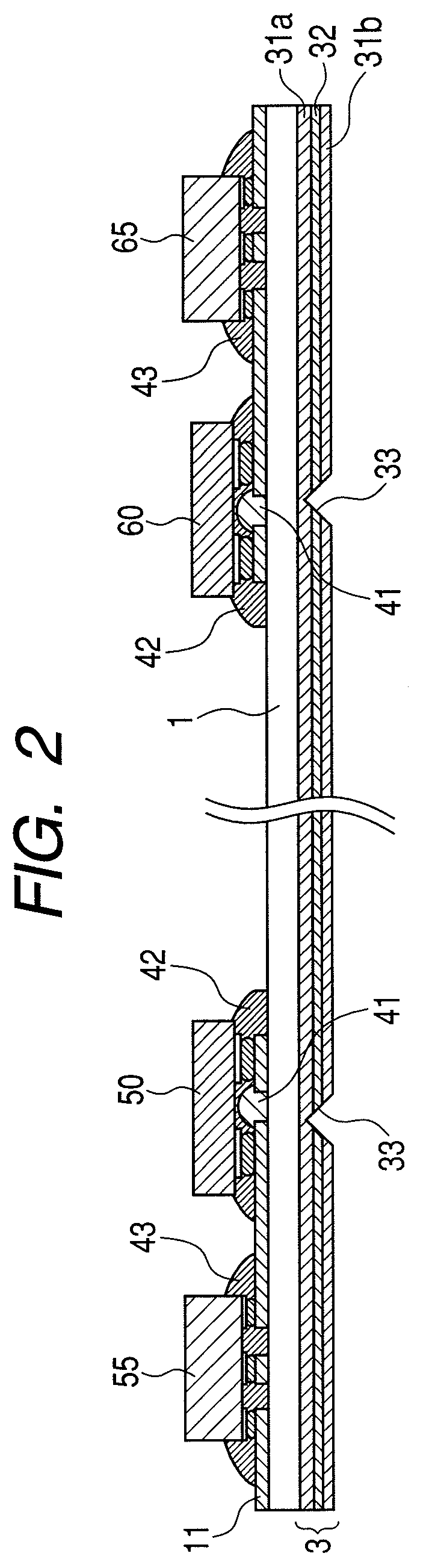
[0029]A junction structure between an optical element and a substrate having a light transmission line, a method of manufacturing an optical module, and an optical wiring device using the junction structure between an optical element and a substrate according to a first embodiment of the present invention are described below with reference to FIGS. 1A to 1E and FIG. 3. FIGS. 1A to 1E are views illustrating a junction structure between an optical element and a substrate using an Au bump and a method of manufacturing an optical module according to the first embodiment. FIG. 2 and FIGS. 3A and 3B are views each illustrating a cross section of a light-transmitting / receiving module which is an optical wiring device using the junction structure between an optical element and a substrate according to the first embodiment. FIG. 1A to FIG. 1D are views each illustrating a cross section of the junction structure between an optical element and a substrate according to the first embodiment. FIG...

second embodiment

[0045]A junction structure between an optical element and a substrate having a light transmission path and a method of manufacturing the light module according to a second embodiment of the present invention will be described below with reference to FIGS. 4A to 4E. FIGS. 4A to 4D are views each illustrating a cross section of the junction structure for an optical element according to the second embodiment, and FIG. 4E is a transparent plan view illustrating the junction structure for an optical element according to the second embodiment. Also in descriptions of the second embodiment, it is assumed that Kapton is used as a polyimide film constituting the substrate 1 and a VCSEL is used as the optical element 2.

[0046]The first embodiment shown in FIGS. 1A to 1E is different from the second embodiment in that an opening 13 is provided in the polyimide film (for instance, Kapton) constituting the substrate 1, as shown in FIGS. 4A to 4E. The under-fill resin 41 not containing a filler is...


PUM

PropertyMeasurementUnit
thicknessaaaaaaaaaa
refractive indexaaaaaaaaaa
melting pointaaaaaaaaaa

Abstract

The present invention provides a junction structure between an optical element and a substrate. The junction structure is formed by supplying an under-fill resin not containing a filler to a portion functioning as a light path for light emitted from or incoming into the optical element on the substrate, then jointing a conductive bump of the optical element to electric wiring on the substrate, and then thermally hardening the under-fill resin not containing a filler to bond the resin not containing a filler to the optical element and to the substrate so that the under-fill resin containing a filler will not enter a space between the optical element and the substrate when the under-fill resin containing a filler is filled in portions other than the light path between the optical element and the substrate.

Description

BACKGROUND OF THE INVENTION[0001]1. Field of the Invention[0002]The present invention relates to a junction structure between an optical element and a substrate having an optical waveguide, an optical transmission / receiving module which is an optical wiring device using the junction structure, and a method of manufacturing an optical module. More specifically, the invention relates to a junction structure between an optical element packaged by means of the flip-chip bonding and a substrate and a method of manufacturing an optical module.[0003]2. Description of the Related Art[0004]Recently, an optical wiring device is used as a high-speed transmission line more and more in place of electric wiring owing to several reasons. The reasons are, for instance, that optical wiring devices are applicable in a high bit rate transmission as compared with the electric wiring, that optical wiring devices are excellent in resistance against noises caused by electromagnetic waves, and that a capac...

Claims


Application Information

Patent Timeline
Patent Type & Authority Applications(United States)
IPC IPC(8): G02B6/12B29D11/00G02B6/26
CPCG02B6/42G02B6/4239G02B6/4214G02B6/4212
Inventor TAKAI, TOSHIAKIMIZUSHIMA, AKIKOMATSUSHIMA, NAOKI
Owner HITACHI CABLE
Why Eureka
Try Eureka