Method of Forming Gate Electrode

a gate electrode and gate oxide technology, applied in the direction of writing connectors, semiconductor devices, printing, etc., can solve the problems of deterioration of the gate oxide layer, and achieve the effect of improving the threshold voltage distribution characteristi

Inactive Publication Date: 2009-07-16
SK HYNIX INC
View PDF7 Cites 3 Cited by
  • Summary
  • Abstract
  • Description
  • Claims
  • Application Information

AI Technical Summary

Benefits of technology

[0005]An object of the present invention is to provide a method of forming a gate electrode, in which a polysilicon layer, which is in contact with a gate insulating layer and has a uniform and densed grain size, is formed to form a gate electrode in which boundaries of the grains being in contact with the gate insulating layer are regularly distributed, whereby a concentration of the dopant on an interface between the gate insulating layer and the gate electrode becomes uniform to improve a threshold voltage distribution characteristic between the gates.

Problems solved by technology

During the process, however, a dopant of the polysilicon is diffused to an interface between the gate electrode and the gate oxide layer along the irregular boundary of the grain so that the gate oxide layer is deteriorated.

Method used


Image

  • Method of Forming Gate Electrode
  • Method of Forming Gate Electrode
  • Method of Forming Gate Electrode

Examples


Embodiment Construction

[0012]Hereinafter, the preferred embodiments of the present invention will be explained in more detail with reference to the accompanying drawings. Hereinafter, the preferred embodiments of the present invention will be explained in more detail with reference to the accompanying drawings. However, it should be understood that the embodiment of the present invention can be variously modified, a scope of the present invention is not limited to the embodiment described herein, and the embodiment is provided for explaining more completely the present invention to those skilled in the art.

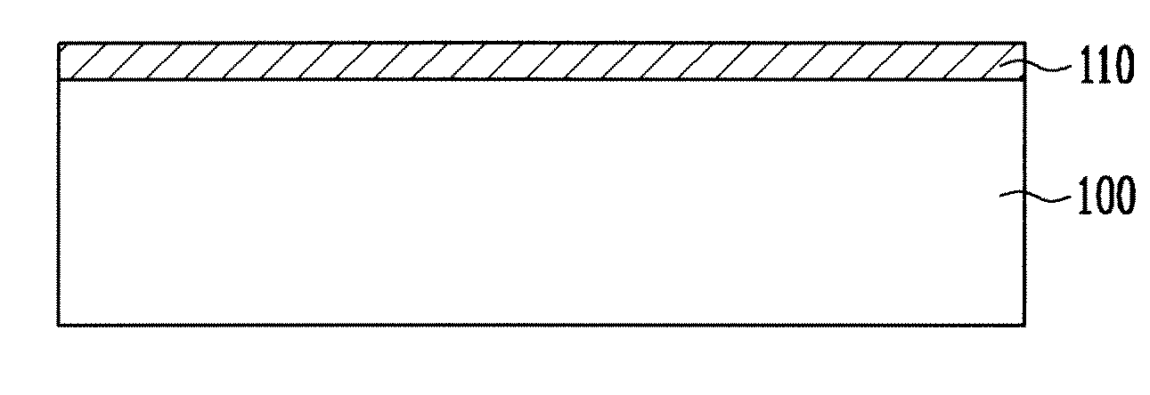
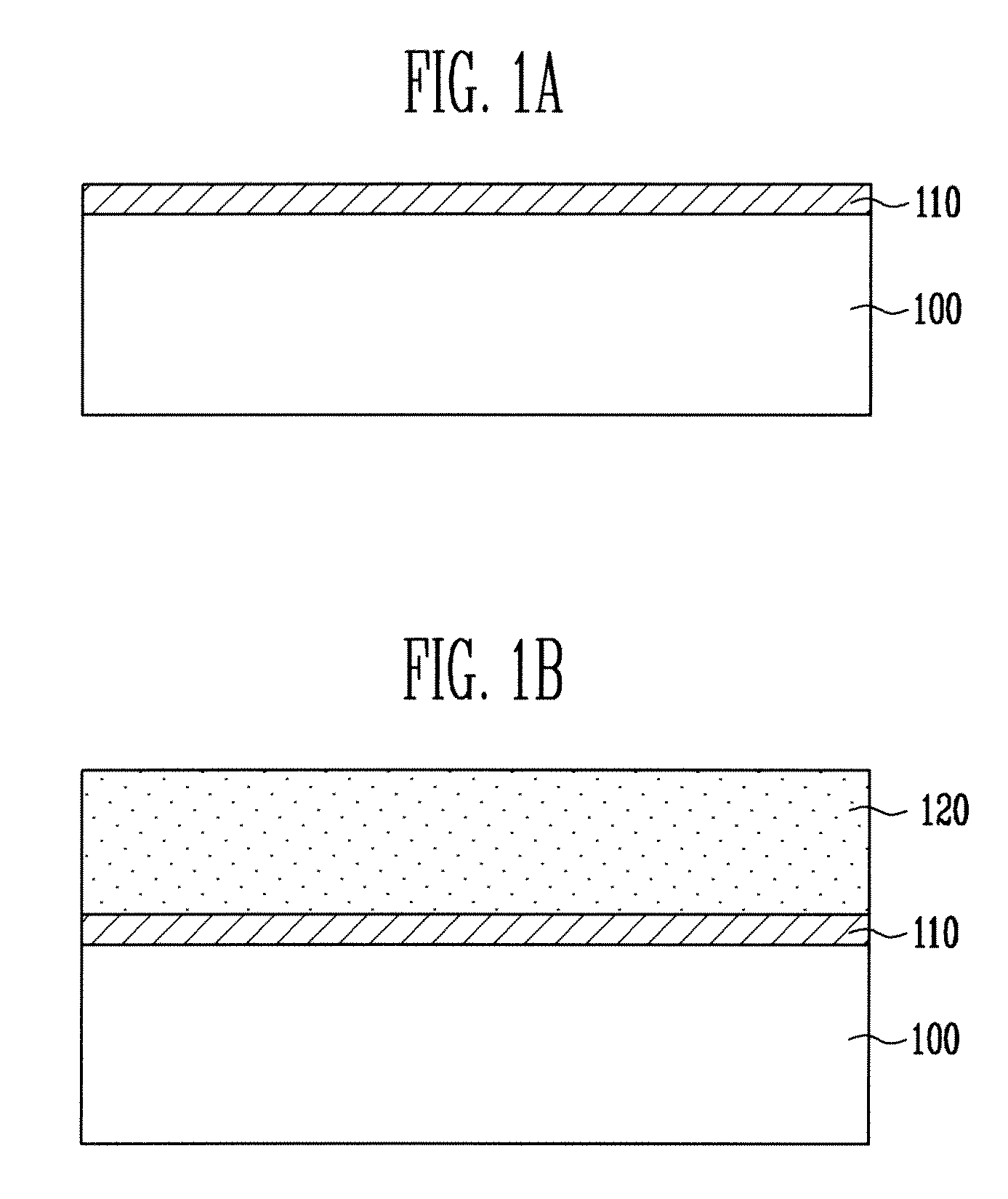
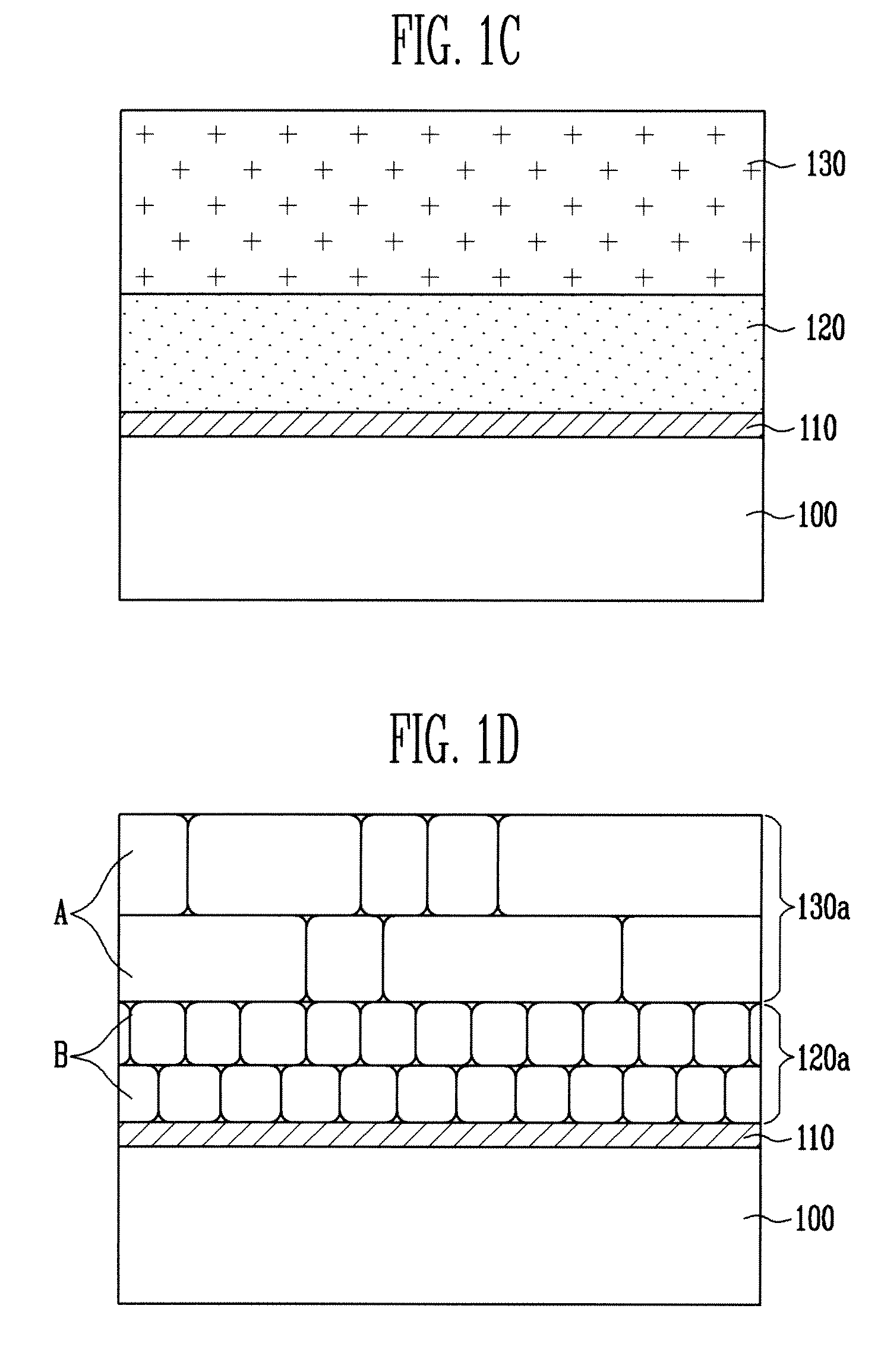
[0013]FIG. 1A to FIG. 1D are sectional views of a device for illustrating a method of forming a gate electrode of a semiconductor device according to one embodiment of the present invention.

[0014]Referring to FIG. 1A, a gate insulating layer 110 is formed on a semiconductor substrate 100. A silicon oxide (SiO2) layer may be formed as the gate insulating layer 110, and an oxidation process may be perform...


PUM

PropertyMeasurementUnit
pressureaaaaaaaaaa
temperatureaaaaaaaaaa

Abstract

The present invention discloses to a method of forming a gate electrode, the method according to the present invention comprises the steps of forming a lower amorphous silicon layer using silane (SiH4) gas and nitrous oxide (N2O) gas; forming an upper amorphous silicon layer on the lower amorphous silicon layer; and crystallizing the lower and upper amorphous silicon layers through a thermal process.

Description

CROSS-REFERENCE TO RELATED APPLICATION[0001]This application claims priority from Korean Patent Application No. 10-2008-0003896, filed on Jan. 14, 2008, the contents of which are incorporated herein by reference in its entirety.BACKGROUND OF THE INVENTION[0002]The present invention relates to a method of forming a gate electrode, more particularly relates to a method of forming a gate electrode, being capable of oxidizing partially a lower amorphous silicon layer to form a lower polysilicon layer which is more uniform and denser than an upper polysilicon layer.[0003]A gate of a semiconductor is formed by stacking a gate electrode on a gate oxide layer. In order to reduce a concentration of an impurity (for example, phosphorous (P)) on an interface between the gate electrode and the gate oxide layer, in general, the gate electrode is formed with a stack layer consisting of an undoped polysilicon layer and a doped polysilicon layer. At this time, a silicon thin layer, which is in amor...

Claims


Application Information

Patent Timeline
Patent Type & Authority Applications(United States)
IPC IPC(8): H01L21/20
CPCH01L21/02576H01L29/4925H01L21/28035H01L21/0262B43K23/001B43K29/00B43M99/008
Inventor PARK, EUN SHILHONG, KWONKIM, JAE HONGKOO, JAE HYOUNG
Owner SK HYNIX INC
Why Eureka
Try Eureka