Ultraviolet sensor and method of manufacturing ultraviolet sensor

a technology of ultraviolet sensor and manufacturing method, which is applied in the field of ultraviolet sensor, can solve the problems of not reaching earth's surface, blackening and inner skin aging in humans, and the inability of ultraviolet sensor for the ultraviolet range of 400 nm or shorter wavelengths to separate detect uv-a and uv-b

Inactive Publication Date: 2009-07-23
LAPIS SEMICON CO LTD
View PDF1 Cites 81 Cited by
  • Summary
  • Abstract
  • Description
  • Claims
  • Application Information

AI Technical Summary

Problems solved by technology

That is, the UV-A wave may cause blackening and inner skin aging in humans.
However, the UV-C is typically absorbed in the ozone layer and thus the vast majority does not

Method used


Image

  • Ultraviolet sensor and method of manufacturing ultraviolet sensor
  • Ultraviolet sensor and method of manufacturing ultraviolet sensor
  • Ultraviolet sensor and method of manufacturing ultraviolet sensor

Examples


Embodiment Construction

[0034]The exemplary embodiments are described and illustrated below to encompass ultraviolet sensors using a photodiode capable of receiving rays containing an ultraviolet ray and generating current, as well as exemplary methods of manufacturing an ultraviolet sensor. Of course, it will be apparent to those of ordinary skill in the art that the embodiments discussed below are exemplary in nature and may be reconfigured without departing from the scope and spirit of the disclosure. However, for clarity and precision, the exemplary embodiments as discussed below may include optional steps, methods, and features that one of ordinary skill should recognize as not being a requisite to fall within the scope of the disclosure.

[0035]Hereinafter, an ultraviolet sensor and a method of manufacturing an ultraviolet sensor will be described with reference to the drawings according to an exemplary embodiment of the disclosure.

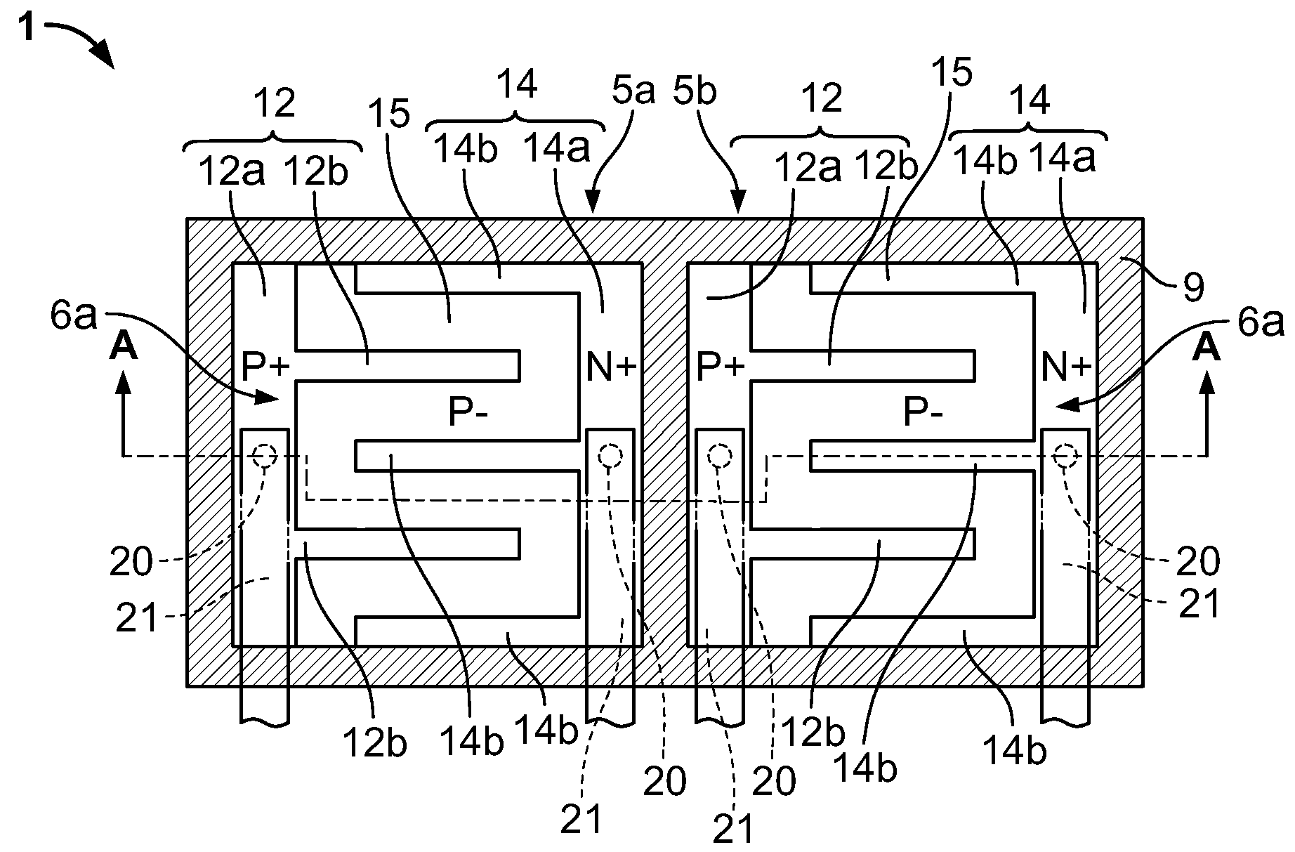
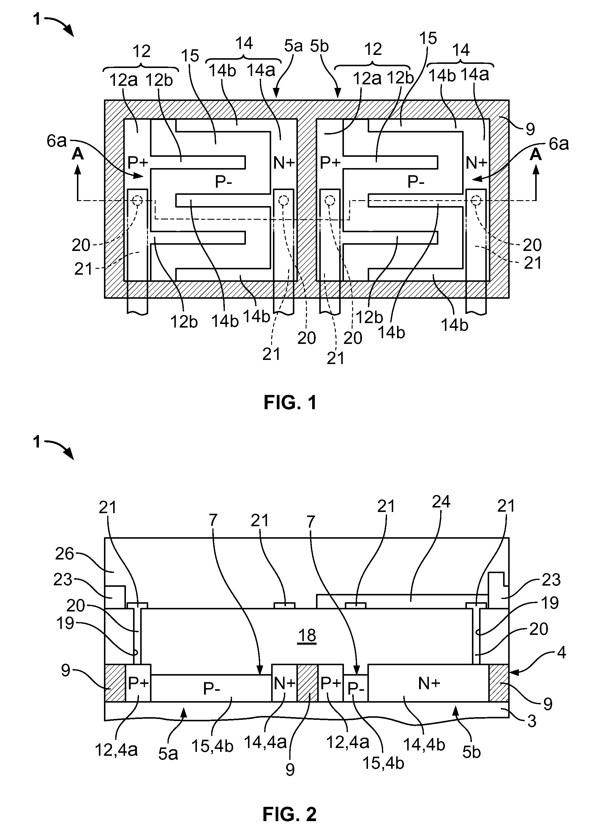
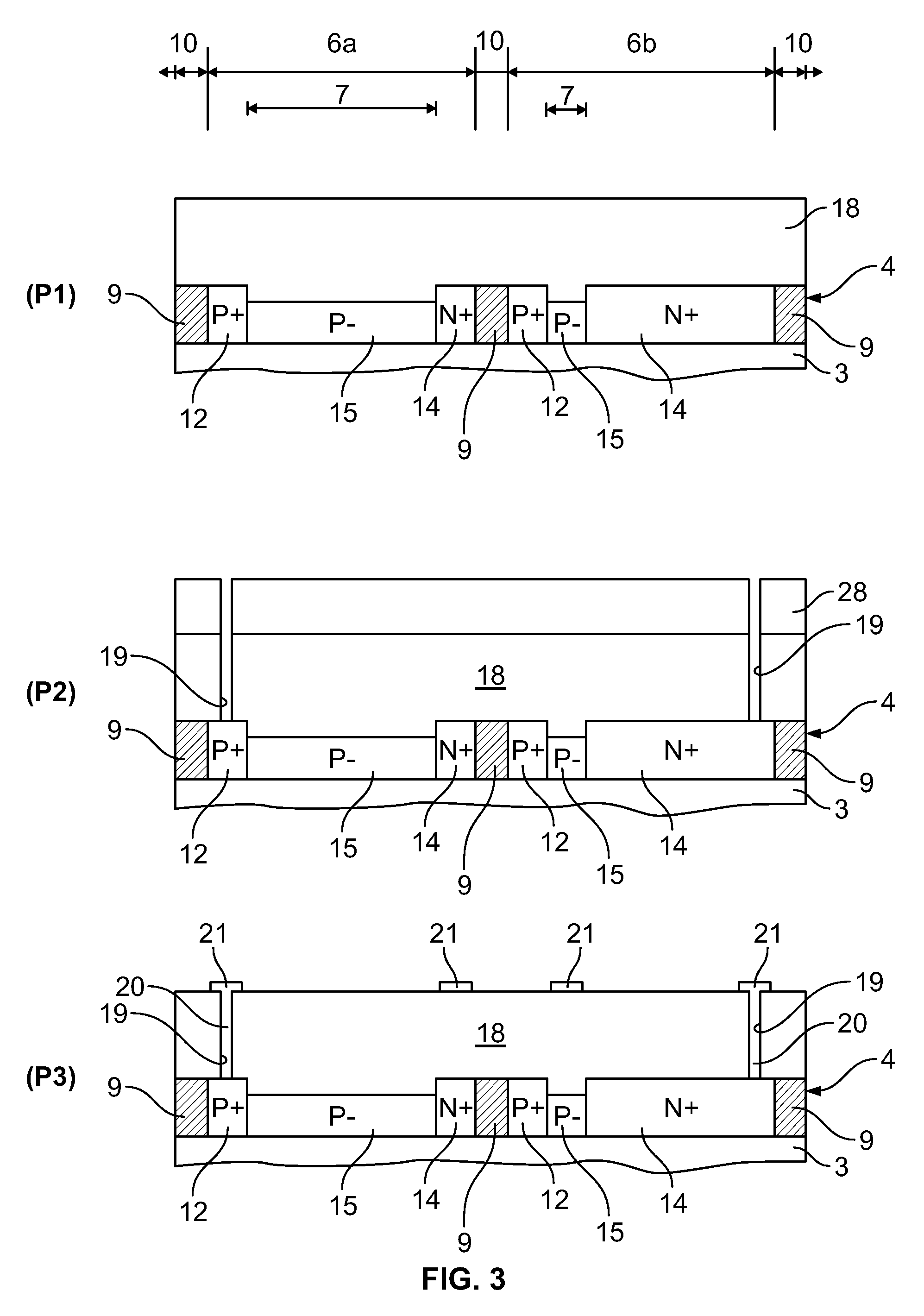
[0036]Referring to FIGS. 1 and 2, an ultraviolet sensor 1 includes a pa...


PUM


Abstract

An ultraviolet sensor capable of separately detecting amount of ultraviolet irradiation of two wavelength range of a UV-A wave and a UV-B wave is provided. The ultraviolet sensor includes: a pair of photodiodes in which a high concentration P-type diffusion layer formed by diffusing a P-type impurity with a high concentration and a high concentration N-type diffusion layer formed by diffusing an N-type impurity with a high concentration, which are formed in a first silicon semiconductor layer on an insulation layer, are opposed to each other with a low concentration diffusion layer, which is formed in a second silicon semiconductor layer thinner than the first silicon semiconductor layer by diffusing one of the P-type impurity or the N-type impurity with a low concentration, interposed therebetween; an interlayer insulation film which is formed on the first and second silicon semiconductor layers; a filter film which is formed on the interlayer insulation layer of one of the photodiodes and formed of a silicon nitride film transmitting rays of a wavelength range of the UV-A wave or a longer wave; and a sealing layer which covers the interlayer insulation film of the other of the photodiodes and the filter film and transmits rays of the wavelength range of the UV-B wave or a longer wave.

Description

CROSS-REFERENCE TO RELATED APPLICATIONS[0001]This application claims priority under 35 U.S.C. §119 to Japanese Patent Application Serial No. JP 2008-011907 filed on Jan. 22, 2008, entitled “ULTRAVIOLET SENSOR AND METHOD OF MANUFACTURING ULTRAVIOLET SENSOR,” the disclosure of which is hereby incorporated by reference.RELATED ART[0002]1. Field of the Invention[0003]The present disclosure relates to an ultraviolet sensor using a photodiode capable of receiving rays containing an ultraviolet ray and generating current, as well as methods of manufacturing an ultraviolet sensor.[0004]2. Description of the Related Art[0005]Known ultraviolet sensors detect the intensity of an ultraviolet ray by forming a photodiode in which an N+ diffusion layer is formed in the pectinate shape of an “E” by diffusing an N-type impurity in a high concentration. Opposing comb portions of a P+ diffusion layer are formed in the pectinate shape of “π” by diffusing a P-type impurity with a high concentration. The...

Claims


Application Information

Patent Timeline
IPC IPC(8): G01J1/42
CPCG01J1/429H01L31/109H01L21/3185H01L21/0217
Inventor MIURA, NORIYUKI
Owner LAPIS SEMICON CO LTD
Why Eureka
Try Eureka