Method and structure for forming trench dram with asymmetric strap

a technology of asymmetric straps and trench drams, which is applied in the direction of instruments, semiconductor devices, computing, etc., can solve the problems of complex and costly prior art methods of forming asymmetric buried straps in trench drams, and essentially increases the process cos

Inactive Publication Date: 2009-07-23
ALSEPHINA INNOVATIONS INC
View PDF6 Cites 34 Cited by
  • Summary
  • Abstract
  • Description
  • Claims
  • Application Information

AI Technical Summary

Problems solved by technology

Prior art methods of forming asymmetric buried strap in a trench DRAM are complicated and costly because they require either a strap mask or deposition, and etch of multiple sacrificial layers.
However, this method is complex and it essentially increases process cost.

Method used


Image

  • Method and structure for forming trench dram with asymmetric strap
  • Method and structure for forming trench dram with asymmetric strap
  • Method and structure for forming trench dram with asymmetric strap

Examples


Embodiment Construction

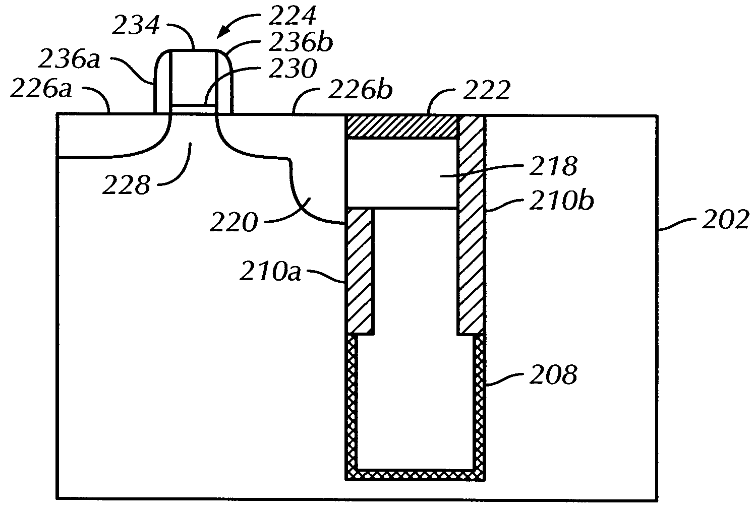
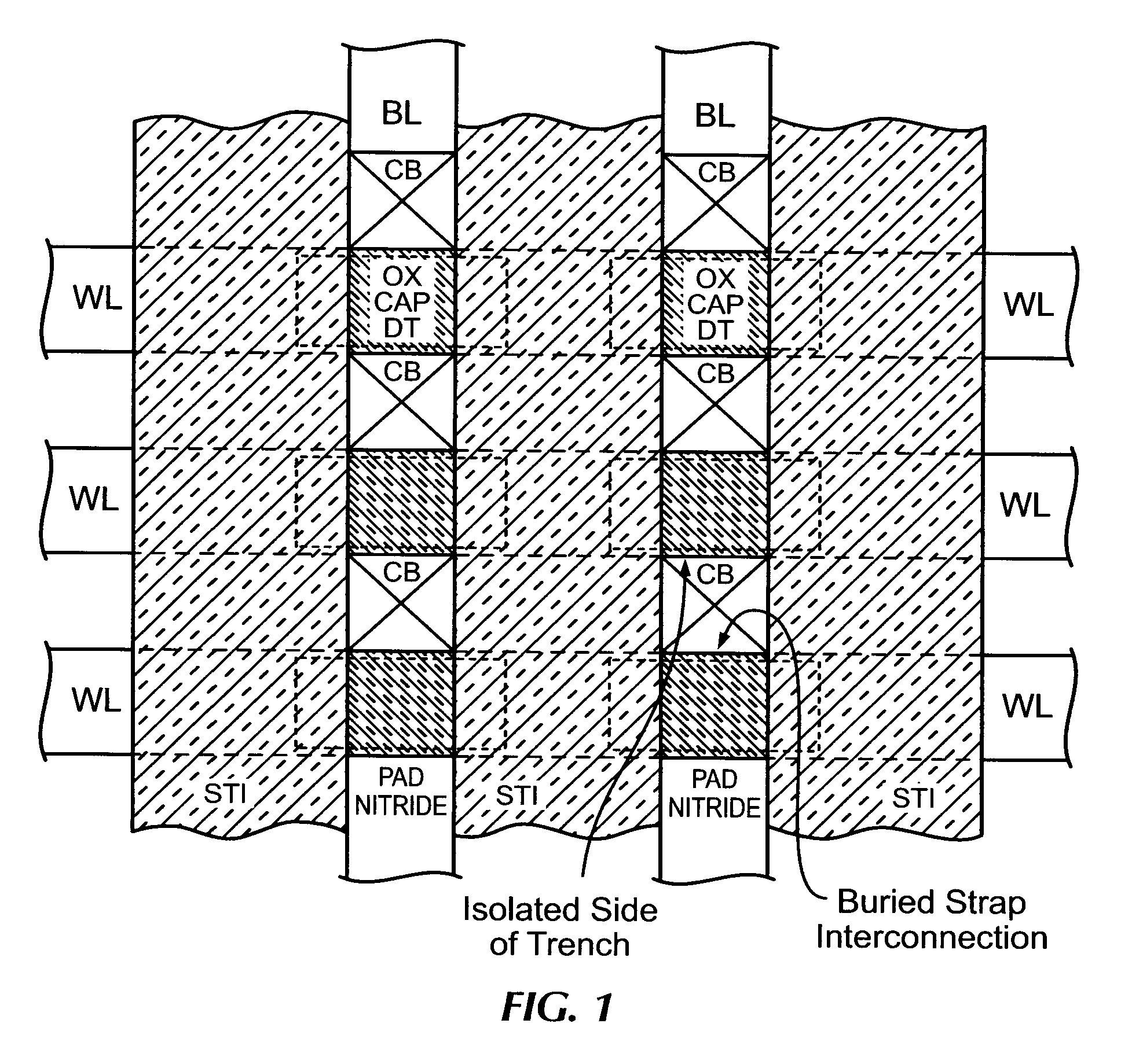
[0019]Referring now to the drawing figures, wherein like references numerals identify identical or corresponding elements, an embodiment of the presently disclosed improved method and structure for forming trench embedded DRAM with asymmetric strap will be disclosed in detail. In the following description, numerous specific details are set forth, such as particular structures, components, materials, dimensions, processing steps and techniques, in order to provide a thorough understanding of the present invention. However, it will be appreciated by one skilled in the art that the invention may be practiced without these specific details. In other instances, well-known structures or processing steps have not been described in detail to avoid obscuring the invention.

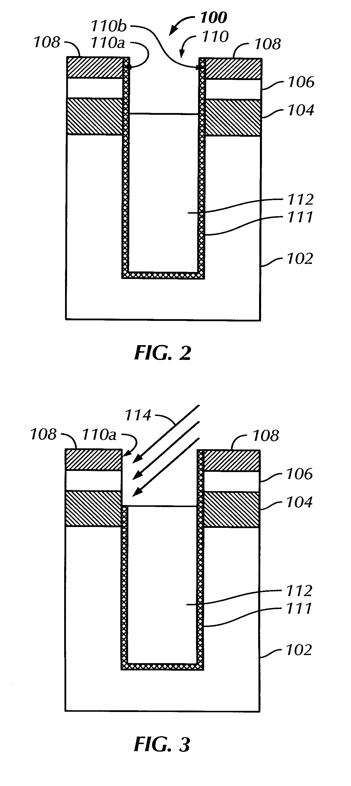
[0020]FIGS. 2-5 illustrate exemplary process steps of forming an asymmetric (i.e. single-sided) strap in a trench embedded DRAM at various stages in accordance with one embodiment of the present disclosure. In particular, t...


PUM


Abstract

A method of forming a trench device structure having a single-side buried strap is provided. The method includes forming a deep trench in a semiconductor substrate, said deep trench having a first side portion and a second side portion; depositing a node dielectric on said deep trench, wherein said node dielectric covers said first side portion and said second side portion; depositing a first conductive layer over said node dielectric; performing an ion implantation or ion bombardment at an angle into a portion of said node dielectric, thereby removing said portion of said node dielectric from said first side portion of said deep trench; and depositing a second conductive layer over said first conductive layer, wherein said second conductive layer outdiffuses into a portion of said semiconductor substrate. A trench device structure having a single-side buried strap is also provided. The device structure includes a semiconductor substrate having a deep trench therein; and a first conductive layer and a second conductive layer sequentially disposed on said deep trench, wherein said second conductive layer outdiffuses into a portion of said semiconductor substrate.

Description

BACKGROUND OF THE INVENTION[0001]1. Technical Field[0002]The present disclosure relates generally to semiconductor memory devices, and, more particularly, to an improved method and structure for forming a deep trench capacitor structure having asymmetric buried strap.[0003]2. Description of Related Art[0004]A dynamic random access memory (DRAM) comprises a capacitor for storing charge and a pass transistor (also called a pass gate, access transistor, or switching transistor) for transferring charge to and from the capacitor. Data (i.e. 1 bit) stored in the cell is determined by the absence or presence of charge on the storage capacitor. In a crosspoint DRAM memory array, bitlines and wordlines crisscross the array and a storage capacitor is accessible at every place where a bitline crosses a wordline. FIG. 1 illustrates an example of such an array in which, the wordlines cross a semiconductor surface along one axis and the bitlines cross the semiconductor surface along a perpendicul...

Claims


Application Information

Patent Timeline
Patent Type & Authority Applications(United States)
IPC IPC(8): H01L21/8239H01L29/92G06F17/50
CPCH01L21/26586H01L29/7833H01L27/10867H10B12/0385
Inventor CHENG, KANGGUOLI, XIWISE, RICHARD
Owner ALSEPHINA INNOVATIONS INC
Why Eureka
Try Eureka