Electrophoretic display panel driving method and electrophoretic display panel

a technology of display panel and electrophoretic particles, which is applied in the direction of static indicating devices, non-linear optics, instruments, etc., can solve the problems of unnecessarily high cost of circuit driving electrophoretic particles whose response speed is lower than that of liquid crystals, and the operation speed of organic tfts is lower than that of a known semiconductor elemen

Inactive Publication Date: 2009-07-23
SEIKO EPSON CORP
View PDF1 Cites 22 Cited by
  • Summary
  • Abstract
  • Description
  • Claims
  • Application Information

AI Technical Summary

Benefits of technology

[0010]An advantage of some aspects of the invention is that it provides an electrophoretic display panel and a method of driving the electrophoretic display panel capable of driving pixels using a semiconductor element which outputs signals of which the number is smaller than the number of scanning lines or the number of data lines in semiconductor elements driving the scanning lines or the data lines formed on an active matrix substrate.

Problems solved by technology

Moreover, a circuit driving the electrophoretic particles of which a response speed is lower than that of liquid crystal is unnecessarily costly.
However, an operation speed of the organic TFTs is lower than that of a known semiconductor element using silicon or the like.
That is, even in the active matrix type circuit which includes the organic TFTs and is formed at low cost by the ink jet process, a problem also occurs when the electrophoretic display panel or the electrophoretic display device needs to be manufactured at low cost in that a known semiconductor driver module has to be used.

Method used


Image

  • Electrophoretic display panel driving method and electrophoretic display panel
  • Electrophoretic display panel driving method and electrophoretic display panel
  • Electrophoretic display panel driving method and electrophoretic display panel

Examples


Embodiment Construction

[0044]Hereinafter, an electrophoretic display panel and a method of driving the electrophoretic display panel will be described with reference to the drawings according to a first embodiment of the invention.

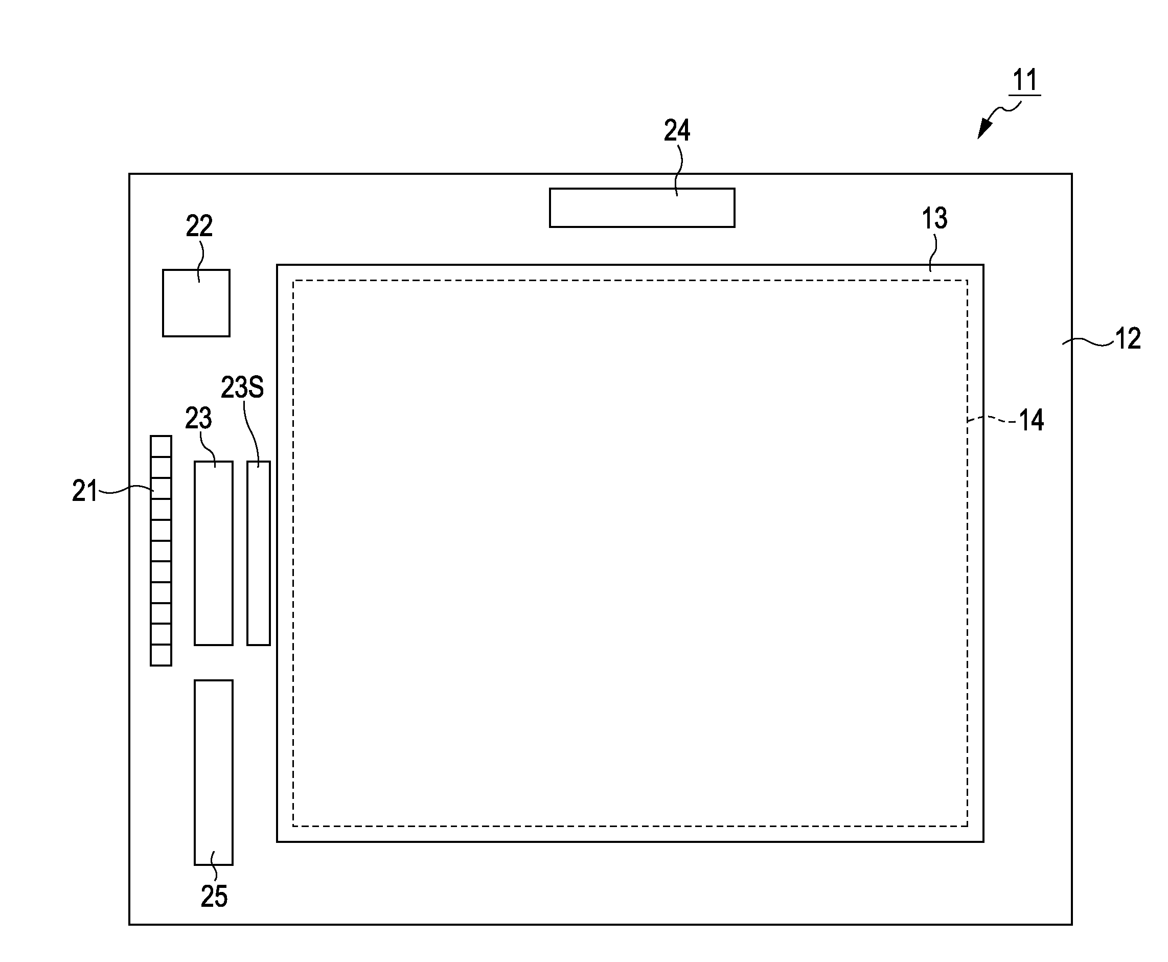
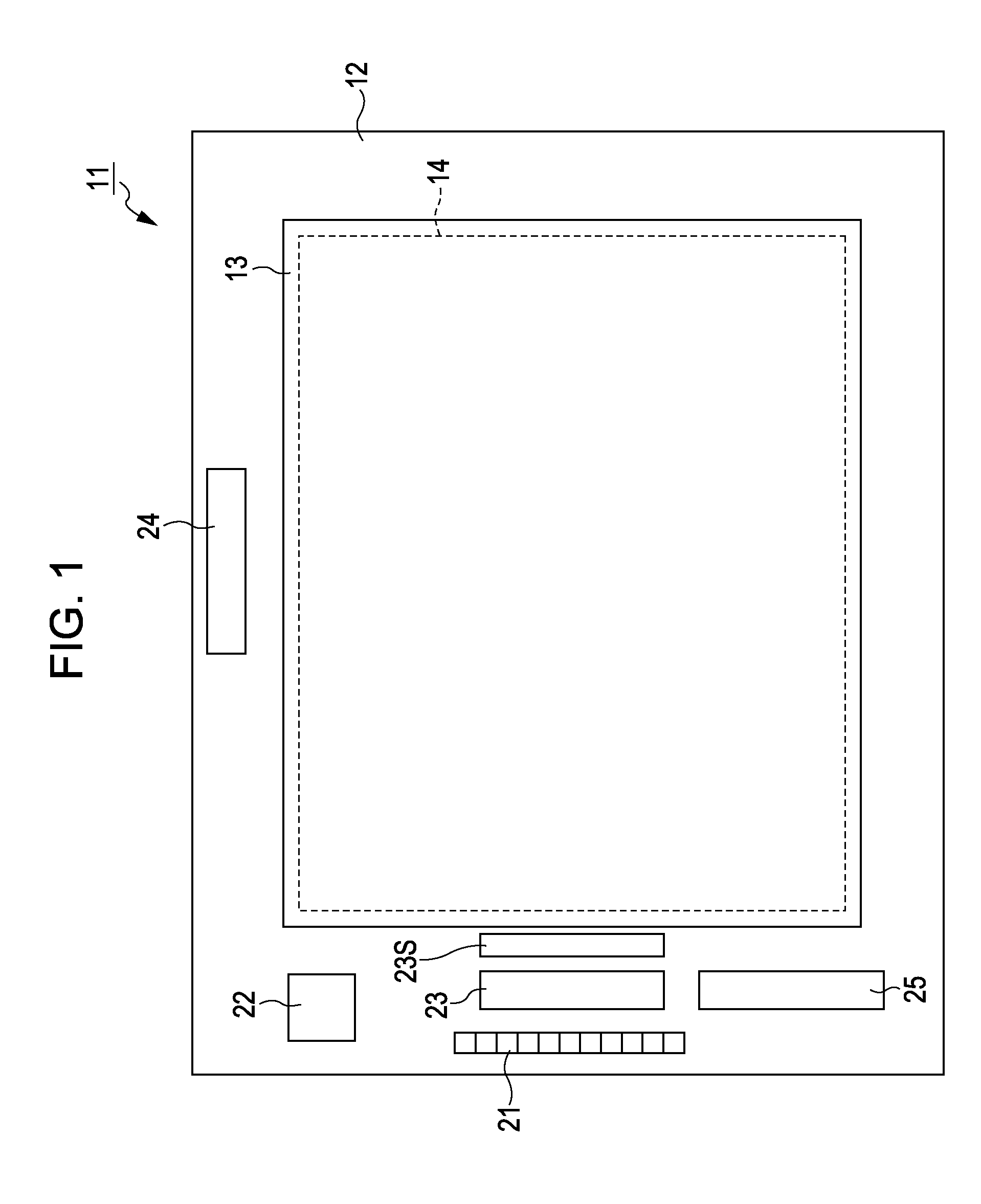
[0045]FIG. 1 is a plan view illustrating the configuration of an electrophoretic display panel (display panel) 11.

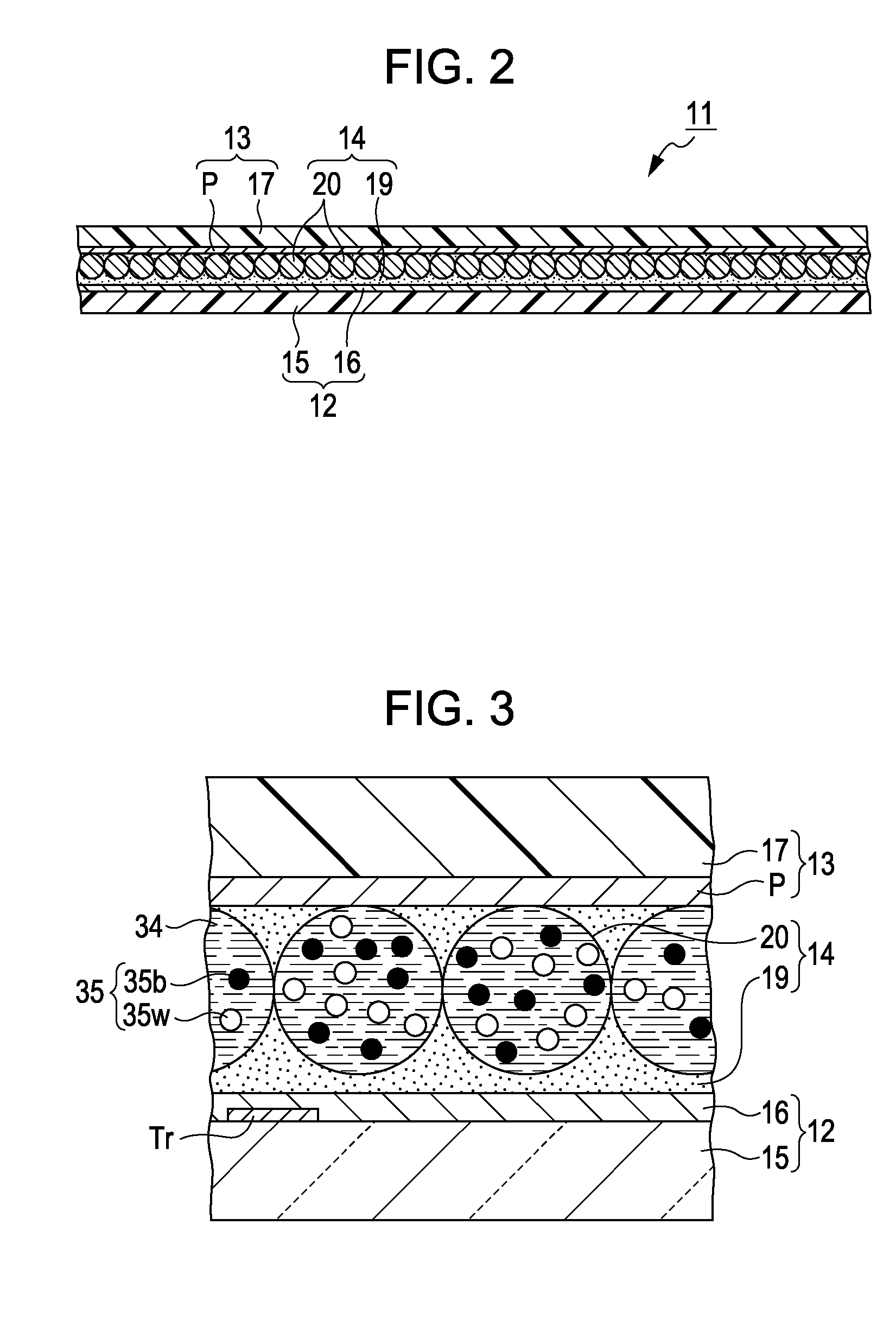
[0046]As shown in FIG. 1, the display panel 11 includes an element substrate 12, a counter substrate 13, and an electrophoretic display layer 14 interposed between the element substrate 12 and the counter substrate 13.

[0047]As shown in FIG. 2, the element substrate 12 includes a rear surface substrate 15 having a flexible property. An element formation layer 16 is formed on one surface (an upper surface in FIG. 2) of the rear surface substrate 15. The rear surface substrate 15 is formed of a thermoplastic resin material or a thermohardening resin having an excellent flexibility and an excellent elasticity, such as polyethylene terephthalate, polycarbonate, polyimide,...


PUM


Abstract

An electrophoretic display panel includes an element substrate, a counter substrate, and an electrophoretic display layer interposed between the element substrate and the counter substrate. The element substrate includes a first data line set including plural data lines, second data line sets each including plural data lines branched from each of the plural data lines of the first data line set, plural scanning lines, and plural pixel electrodes. The plural pixel electrodes are disposed at locations where the plural data lines of the second data line sets intersect with the plural scanning lines. The counter substrate includes plural common electrodes, and one or more common electrodes is disposed opposite the plural pixel electrodes corresponding to one of the second data line sets.

Description

BACKGROUND[0001]1. Technical Field[0002]The present invention relates an electrophoretic display panel driving method and an electrophoretic display panel.[0003]2. Related Art[0004]In recent years, as a display device used in an apparatus such as an electronic paper or an electronic poster which needs a flexible property, non-luminescent type display devices having a flexible structure were used. One of the non-luminescent type display devices is an electrophoretic display device using an electrophoresis phenomenon. Here, the electrophoresis phenomenon is a phenomenon that particles (electrophoretic particles) migrate by the Coulomb force upon applying an electric field to a dispersal system in which the particles are dispersed in a fluid (dispersion medium). The electrophoretic display device is driven by changing potential between electrodes opposed to each other with the electrophoretic particles interposed therebetween by drive of thin film transistors and causing an electric fi...

Claims


Application Information

Patent Timeline
Patent Type & Authority Applications(United States)
IPC IPC(8): G09G3/30
CPCG02F1/167G02F2001/134318G02F2001/1676G02F2201/121G02F2201/122G09G2380/02G09G3/3655G09G2300/0426G09G2310/0218G09G2310/0267G09G3/344G09G3/035G02F1/134318G02F1/16766G02F1/1685
Inventor MIYAMOTO, TSUTOMU
Owner SEIKO EPSON CORP
Why Eureka
Try Eureka