Substrate processing apparatus

Inactive Publication Date: 2009-07-30
TOKYO ELECTRON LTD
View PDF8 Cites 3 Cited by
  • Summary
  • Abstract
  • Description
  • Claims
  • Application Information

AI Technical Summary

Benefits of technology

[0020]In accordance with the present invention, the processing vessel is provided with a baffle plate so that a chamber where the catalyst is present is partitioned from a chamber used for substrate processing by hydrogen radicals. In this way, products from the substrate process are prevented from approaching the catalyst and the catalyst is protected against degradation. Especially, when the substrate processing involves a resist ashing process, carbon-containing materials separated from the resist the catalyst and carbonize the surface of the resist. This resultantly degrades catalyst performance, or shorten

Problems solved by technology

However, the combined dry ashing and wet ashing approach makes the manufacturing process more complicated and takes more time.
In addition, when the deteriorated resists are peeled off, undesirable residues can be remained on an underlayer of the resists, which require an additional process to clean them.
However, it has been found t

Method used


Image

  • Substrate processing apparatus
  • Substrate processing apparatus
  • Substrate processing apparatus

Examples


Example

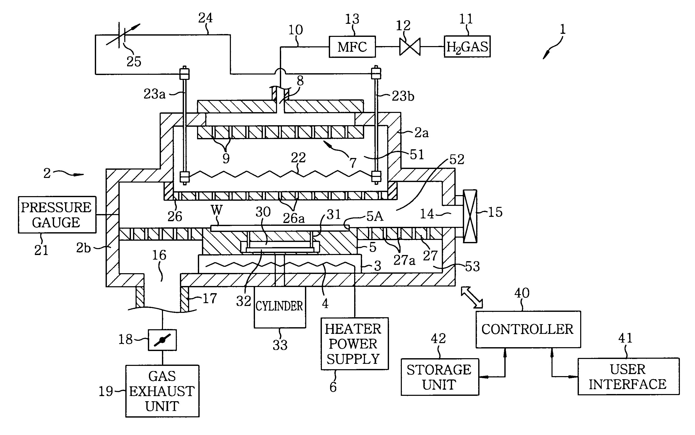
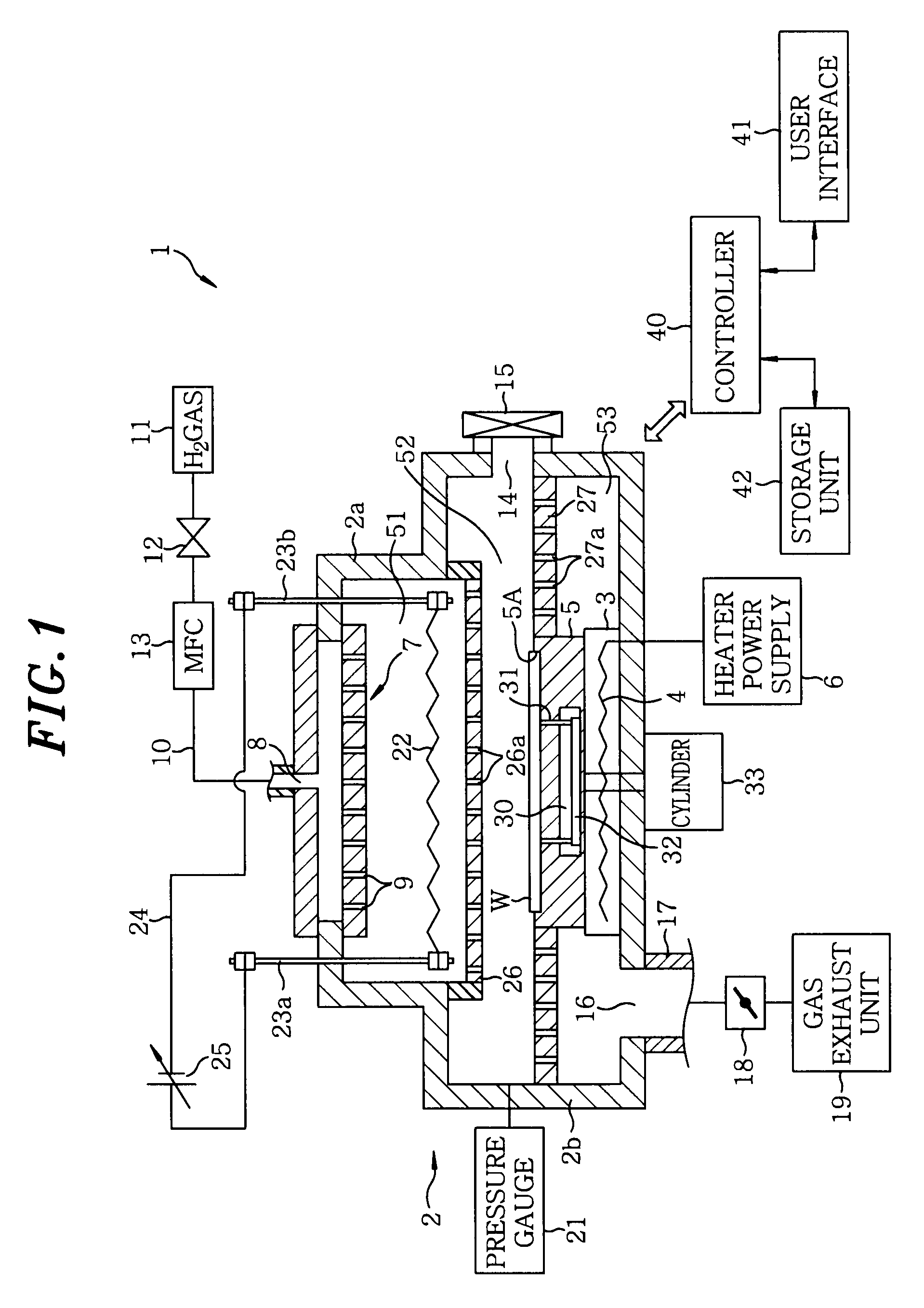
[0037]First, a first embodiment of the present invention will be described. FIG. 1 is a cross-sectional view showing a substrate processing apparatus in accordance with the first embodiment of the present invention.

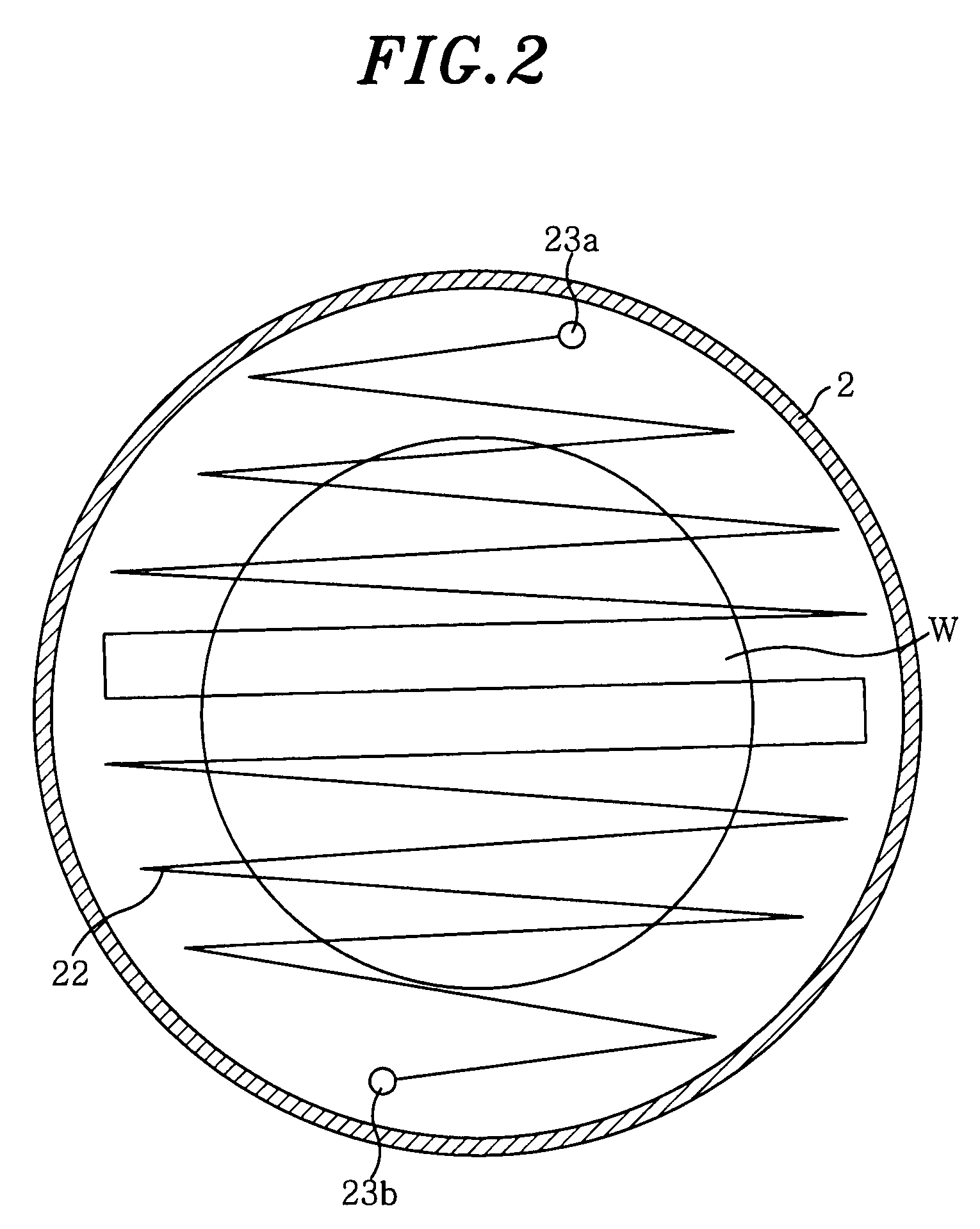
[0038]A substrate processing apparatus 1 is configured as a resist peeling (ashing) apparatus, and has an evacuative chamber (processing vessel) 2. The chamber 2 includes an upper portion 2a of a small diameter and a lower portion 2b of a large diameter. Placed on the bottom of the lower portion 2b is a heater plate 3 having a heater 4 buried therein, and a wafer stage 5 to mount thereon a semiconductor wafer (hereinafter, simply referred to as a wafer) W is placed on the heater plate 3, the wafer being served as a target substrate to be processed having a resist film to be peeled off. A recess 5a for mounting the wafer W thereon is formed on the top surface of the wafer stage 5. The heater 4 is electrically fed from a heater power supply 6.

[0039]The wafer stage 5 has a s...

Example

[0078]Hereinafter, a second embodiment of the present invention will be described in detail.

[0079]FIG. 11 is a cross-sectional view showing a substrate processing apparatus in accordance with the second embodiment of the present invention, and FIG. 12 shows an arrangement pattern of a catalyst wire in the substrate processing apparatus in FIG. 11. Like elements between FIG. 1 and FIGS. 11 to 12 are indicated by like reference numerals, and explanations thereof will be omitted. In the substrate processing apparatus 1 of the present embodiment, a disk-shaped guide member 61 is provided directly underneath a gas inlet port 8 for guiding H2 gas introduced through the gas inlet port 8 in outer peripheral direction, and the H2 gas is discharged in a circular shape into the chamber 2 through a discharge port 62 formed between the guide member 61 and the ceiling wall of the chamber 2. Further, as illustrated in FIG. 12, a catalyst wire 22′ of a circular shape is disposed directly underneath...


PUM


Abstract

A substrate processing apparatus includes a processing vessel; a mounting table for mounting the substrate thereon in the processing vessel; a gas inlet unit provided in the processing vessel; a gas supply mechanism for supplying a hydrogen-containing gas into the processing vessel through the gas inlet unit; a gas discharge port provided at the processing vessel; a gas exhaust mechanism for exhausting an inside of the processing vessel through the gas discharge port; a catalyst provided in the processing vessel; and a heating unit for heating the catalyst. Hydrogen radicals are formed in the processing vessel by a catalytic cracking reaction between the hydrogen-containing gas and the catalyst of high temperature, and the substrate is processed by the hydrogen radicals.

Description

FIELD OF THE INVENTION[0001]The present invention relates to a substrate processing apparatus for peeling off a remaining resist on a substrate by a hydrogen gas that is produced by bringing a hydrogen-containing gas into contact with a high temperature catalyst.BACKGROUND OF THE INVENTION[0002]In a manufacturing process of semiconductor devices, a photoresist pattern is formed by performing photolithography on a semiconductor wafer as a target substrate to be processed. The formed photoresist pattern is then used as a mask for etching and is peeled off after etching.[0003]As for the photoresist peeling process, a dry ashing technique using a plasma and a wet ashing technique are the mainstream. Particularly, the dry ashing technique and the wet ashing technique are used in combination to peel resists that are deteriorated after performing ion implantation. However, the combined dry ashing and wet ashing approach makes the manufacturing process more complicated and takes more time. ...

Claims


Application Information

Patent Timeline
IPC IPC(8): B05C13/00B01J19/00
CPCH01L21/67109H01L21/67017
Inventor SAKURAGI, ISAMUTAHARA, SHIGERUYAMAZAKI, KUMIKONONAKA, RYOTAKANASHI, MORIHIRONISHIMURA, EIICHI
Owner TOKYO ELECTRON LTD
Why Eureka
Try Eureka