
Manufacturing process of semiconductor device and semiconductor device

a manufacturing process and semiconductor technology, applied in semiconductor devices, semiconductor/solid-state device details, electrical devices, etc., can solve the problems of increasing the surface temperature of the semiconductor substrate, affecting and the breakage of the semiconductor elements, so as to reduce the manufacturing cost of the semiconductor device and improve the manufacturing yield of the semiconductor devi

Active Publication Date: 2009-07-30
TESSERA ADVANCED TECH
View PDF12 Cites 46 Cited by
  • Summary
  • Abstract
  • Description
  • Claims
  • Application Information

AI Technical Summary

Benefits of technology

[0010]An object of the present invention is to provide a technique capable of reducing the manufacturing cost of a semiconductor device having a through electrode.
[0011]Another object of the present invention is to provide a technique capable of improving the manufacturing yield of a semiconductor device having a through electrode.
[0017]The manufacturing cost of a semiconductor device having a through electrode can be reduced. Also, since the through electrode can be formed without breaking semiconductor elements, the manufacturing yield of a semiconductor device having a through electrode can be improved.

Problems solved by technology

For example, problems such as the increase of the surface temperature of the semiconductor substrate and the breakage of the semiconductor elements by the plasma field are caused.
However, since at least two steps of grinding the semiconductor substrate and removing the insulating film at the bottom of the through hole are required for grinding the rear surface of the semiconductor substrate, it takes long time and there is a fear of the cost increase.

Method used


Image

  • Manufacturing process of semiconductor device and semiconductor device
  • Manufacturing process of semiconductor device and semiconductor device
  • Manufacturing process of semiconductor device and semiconductor device

Examples


first embodiment

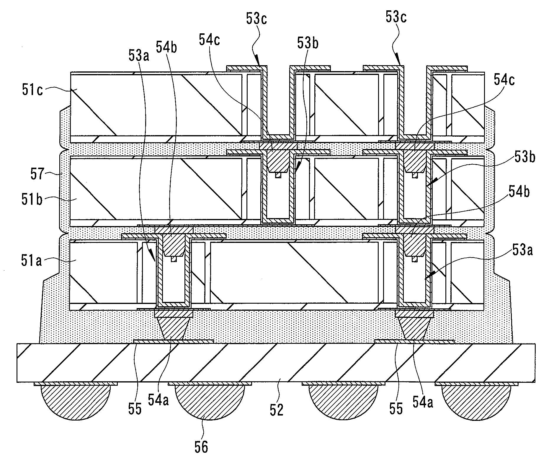
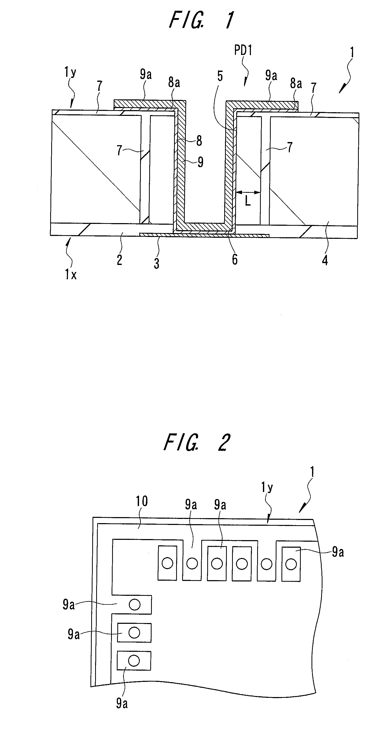
[0044]A through electrode of a semiconductor device according to the first embodiment will be described with reference to FIG. 1 and FIG. 2. FIG. 1 is a cross-sectional view of the principal part of the through electrode of the semiconductor device, and FIG. 2 is a plan view of the principal part of the through electrode of the semiconductor device.

[0045]As shown in FIG. 1, a through electrode PD1 includes a first electrode (element surface electrode 3) formed on a first surface 1x side of a semiconductor wafer 1, a second electrode (pad electrode 9a) formed on a second surface 1y side opposite to the first surface 1x, and a third electrode (contact electrode 9) which electrically connects the first and second electrodes and is formed so as to penetrate through a semiconductor substrate 4 as a base material of the semiconductor wafer 1.

[0046]A semiconductor element (not shown) and a surface protection insulating film (first insulating film) 2 covering the semiconductor element are f...

second embodiment

[0067]A through electrode of a semiconductor device according to the second embodiment will be described with reference to FIG. 18. FIG. 18 is a cross-sectional view of the principal part of the through electrode of the semiconductor device.

[0068]The difference from the above-described first embodiment is that the element surface electrode 3 formed on the first surface 1x side of the semiconductor wafer and the contact electrode 9 formed in the semiconductor substrate 4 are electrically connected via a plurality of contact plugs 22. More specifically, in the through electrode PD1 according to the first embodiment described above, the element surface electrodes 3 formed on the first surface 1x side of the semiconductor wafer and the contact electrode 9 formed in the semiconductor substrate 4 are directly connected by forming the opening 6 having the same diameter as the through hole 5 in the surface protection insulating film 2. In the through electrode PD2 according to the second em...

third embodiment

[0070]A through electrode of a semiconductor device according to the third embodiment will be described with reference to FIG. 19. FIG. 19 is a cross-sectional view of the principal part of the through electrode of the semiconductor device.

[0071]The difference from the above-described first embodiment is that the element surface electrode 3 formed on the first surface 1x side of the semiconductor wafer and the contact electrode 9 formed in the semiconductor substrate 4 are electrically connected via a plurality of contact plugs 22 and an inner electrode (fourth electrode) 23. More specifically, in the through electrode PD1 according to the first embodiment described above, the element surface electrode 3 formed on the first surface 1x side of the semiconductor wafer and the contact electrode 9 formed in the semiconductor substrate 4 are directly connected by forming the opening 6 having the same diameter as the through hole 5 in the surface protection insulating film 2. In the throu...


PUM


Abstract

After forming a ring-shaped trench penetrating through a semiconductor substrate from a rear surface side thereof and forming an insulating film inside the trench and on the rear surface of the semiconductor substrate, a through hole is formed in the insulating film and semiconductor substrate on an inner side of the ring-shaped trench from the rear surface side, thereby exposing a surface protection insulating film formed on a front surface of the semiconductor substrate at a bottom of the through hole. After removing the surface protection insulating film at the bottom of the through hole to form an opening to expose an element surface electrode, a contact electrode connected to the element surface electrode is formed on inner walls of the through hole and opening, and a pad electrode made of the same layer as the contact electrode is formed on the rear surface of the semiconductor substrate.

Description

CROSS-REFERENCE TO RELATED APPLICATION[0001]The present application claims priority from Japanese Patent Application No. JP 2008-017141 filed on Jan. 29, 2008, the content of which is hereby incorporated by reference into this application.TECHNICAL FIELD OF THE INVENTION[0002]The present invention relates to a manufacturing technique of a semiconductor device and a semiconductor device, and more particularly to a technique effectively applied to a manufacturing process of a semiconductor device in which a plurality of semiconductor chips are three-dimensionally stacked.BACKGROUND OF THE INVENTION[0003]With the size reduction of electronic equipment, higher integration and further size reduction of a semiconductor device to be mounted therein have been required. Therefore, the system-in-package technology for densely packaging a plurality of semiconductor chips having integrated circuits formed therein and realizing a high-performance system in a short period of time has attracted at...

Claims


Application Information

Patent Timeline
IPC IPC(8): H01L23/48H01L21/768
CPCH01L21/6835H01L2224/05572H01L23/481H01L24/16H01L24/83H01L24/90H01L25/0657H01L25/50H01L2221/68372H01L2224/1134H01L2224/13025H01L2224/13099H01L2224/16145H01L2224/16225H01L2224/16237H01L2224/73204H01L2224/838H01L2225/06513H01L2225/06517H01L2225/06541H01L2924/01022H01L2924/01078H01L2924/01079H01L2924/14H01L21/76898H01L2924/0002H01L2924/00013H01L2924/01005H01L2924/01006H01L2924/01019H01L2924/01024H01L2924/01033H01L2924/014H01L2924/00014H01L2224/0401H01L2224/16147H01L2224/81191H01L2224/81141H01L21/7682H01L2224/0557H01L2224/05571H01L2924/00012H01L2224/05552
Inventor YOSHIMURA, YASUHIROTANAKA, NAOTAKAKAWASHITA, MICHIHIRONAITO, TAKAHIROAKAZAWA, TAKASHI
Owner TESSERA ADVANCED TECH
Features
  • Generate Ideas
  • Intellectual Property
  • Life Sciences
  • Materials
  • Tech Scout
  • Unparalleled Data Quality
  • Higher Quality Content
  • 60% Fewer Hallucinations
Learn More