Semiconductor chip and semiconductor device

a semiconductor chip and semiconductor technology, applied in semiconductor devices, semiconductor/solid-state device details, electrical devices, etc., can solve the problems of increasing the temperature erroneous operation of the semiconductor device, and inability to radiate heat, so as to suppress the temperature increase of the semiconductor chip, efficiently transmit heat generated, and efficiently radiate heat

Active Publication Date: 2009-07-30
PANASONIC SEMICON SOLUTIONS CO LTD
View PDF15 Cites 12 Cited by
  • Summary
  • Abstract
  • Description
  • Claims
  • Application Information

AI Technical Summary

Benefits of technology

[0005]However, a conventional semiconductor chip as described above has the following problem. With semiconductor devices, there are demands not only for a reduction in size but also for an increase in performance. Therefore, it is required to form a plurality of elements that pass large currents therethrough, such as amplifier elements, in a semiconductor chip. Elements that pass large currents therethrough generate large amounts of heat, thereby increasing the temperature of the semiconductor chip.
[0008]The present invention solves the problem in the prior art and realizes a semiconductor chip capable of efficiently radiating heat from the reverse surface of the semiconductor substrate.
[0011]The semiconductor chip of the present invention includes the heat-radiating plug, whereby it is possible to efficiently transmit heat generated from the semiconductor element to the reverse surface of the substrate. By connecting the heat-radiating plug to a heat-radiating portion of a circuit board, it is possible to efficiently radiate heat and to thereby suppress the temperature increase of the semiconductor chip. Thus, it is possible to improve the reliability of the semiconductor chip. Since the interval between the semiconductor elements can be reduced, it is also possible to reduce the area of the semiconductor chip. Since the heat-radiating plug is electrically insulated from the integrated circuit, the heat-radiating plug will not affect the operation of the integrated circuit.

Problems solved by technology

However, a conventional semiconductor chip as described above has the following problem.
Elements that pass large currents therethrough generate large amounts of heat, thereby increasing the temperature of the semiconductor chip.
Such an increase in the leak current causes an erroneous operation of a semiconductor device.
With a conventional semiconductor chip, however, heat cannot be radiated except via the semiconductor substrate, failing to realize an efficient heat radiation and thus deteriorating the operation reliability.

Method used


Image

  • Semiconductor chip and semiconductor device
  • Semiconductor chip and semiconductor device
  • Semiconductor chip and semiconductor device

Examples


Embodiment Construction

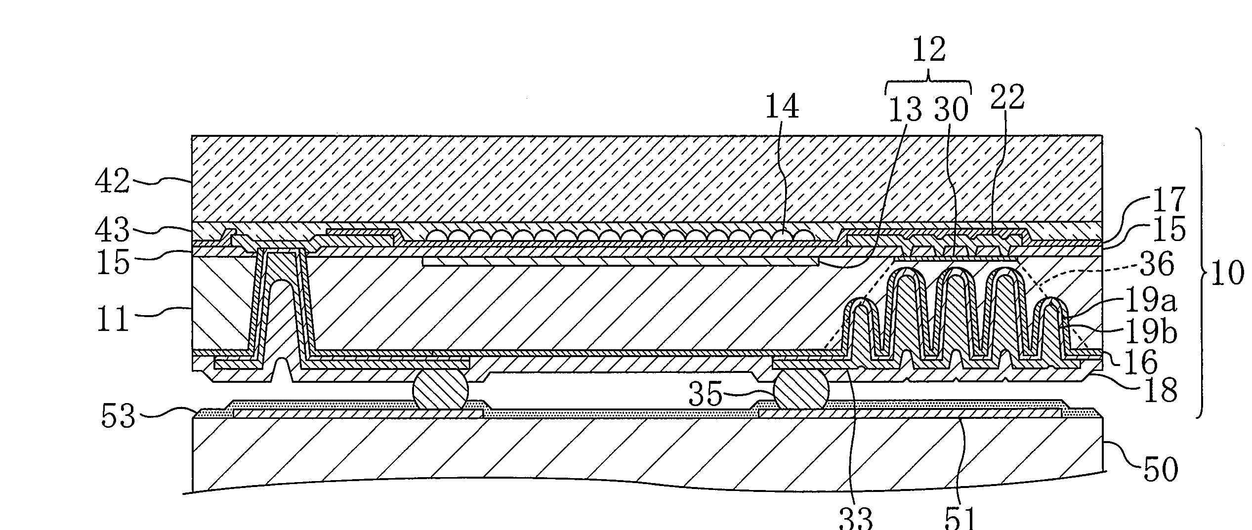
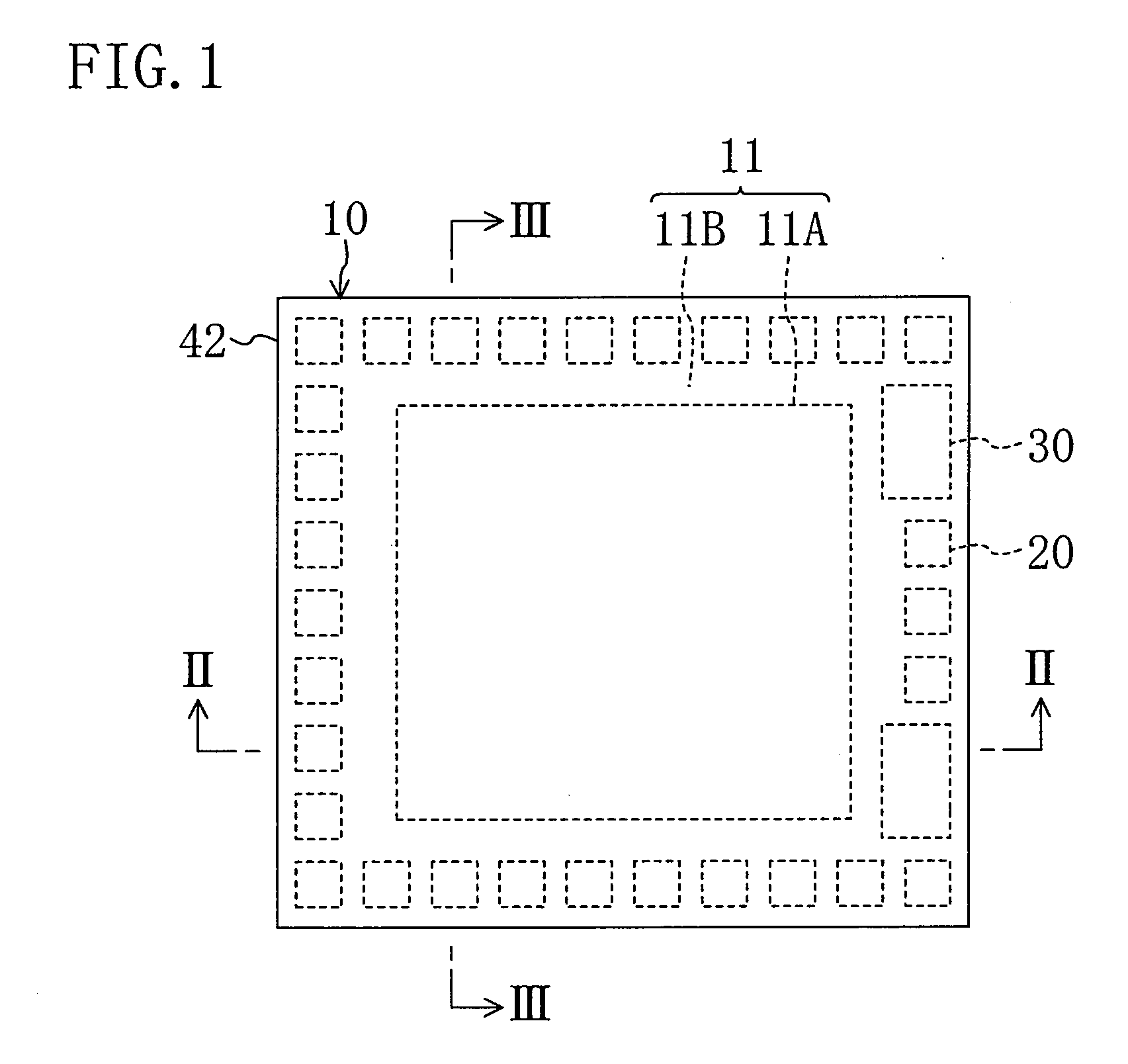
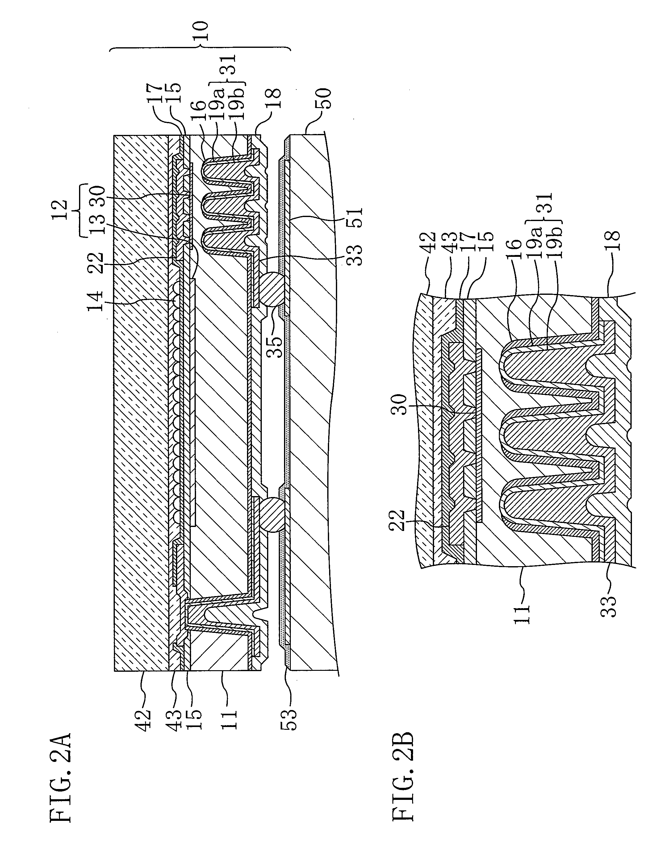
[0016]An embodiment of the present invention will be described with reference to the drawings. FIGS. 1 to 3B show a semiconductor chip according to an embodiment of the present invention, wherein FIG. 1 is a plan view, FIGS. 2A and 2B are cross-sectional views taken along line II-II in FIG. 1, and FIGS. 3A and 3B are cross-sectional views taken along line III-III in FIG. 1. FIG. 2B is an enlarged view of a part of the structure shown in FIG. 2A, and FIG. 3B is an enlarged view of a part of the structure shown in FIG. 3A.

[0017]Referring to FIGS. 1, 3A and 3B, an integrated circuit 12 including a plurality of semiconductor elements is formed on the front surface (i.e., the surface on which semiconductor elements are formed) of a silicon substrate 11. The integrated circuit of the present embodiment is an image-sensing circuit including a plurality of light-receiving elements 13 formed in a light-receiving element region 11A provided in a central portion of the substrate 11. A peripher...


PUM


Abstract

A semiconductor chip, including: a substrate including an front surface; an integrated circuit formed on the front surface and including a plurality of semiconductor elements; and a heat-radiating plug formed in a region of the substrate corresponding to at least one of the semiconductor elements. The heat-radiating plug is made of a material having a thermal conductivity greater than that of the substrate formed in a non-penetrating hole having its opening on a reverse surface of the substrate.

Description

CROSS REFERENCE TO RELATED APPLICATION[0001]This application claims priority under 35 U.S.C. §119 on Patent Application No. 2008-018641 filed in Japan on Jan. 30, 2008, the entire contents of which are hereby incorporated by reference.BACKGROUND OF THE INVENTION[0002]The present disclosure relates to a semiconductor chip and a semiconductor device and, more particularly, to a semiconductor chip including a heat-generating element such as an amplifier element, and a semiconductor device using the same.[0003]Recent electronic devices often use a semiconductor chip including various semiconductor elements integrated therein in order to thereby increase the productivity or reduce the overall size. For example, such a semiconductor chip includes a semiconductor substrate, and an integrated circuit including a plurality of semiconductor elements formed on the front surface of the semiconductor substrate. Such a semiconductor chip includes a connection electrode on the reverse surface for ...

Claims


Application Information

Patent Timeline
Patent Type & Authority Applications(United States)
IPC IPC(8): H01L23/34
CPCH01L23/3677H01L2224/0401H01L27/14618H01L27/14621H01L27/14627H01L27/14636H01L2224/16225H01L2224/05H01L2224/02372H01L2224/05548H01L2224/06181H01L2224/13022H01L2224/13024H01L2224/16227H01L2224/131H01L23/481H01L2924/014H01L2224/02351
Inventor SANO, HIKARITOMITA, YOSHIHIRONAKANO, TAKAHIRO
Owner PANASONIC SEMICON SOLUTIONS CO LTD
Why Eureka
Try Eureka