MEMS micromirror devices with Anti-reflective structures

Active Publication Date: 2009-07-30
LUMENTUM OPERATIONS LLC
View PDF4 Cites 13 Cited by
  • Summary
  • Abstract
  • Description
  • Claims
  • Application Information

AI Technical Summary

Benefits of technology

[0011]In accordance with the invention there is provided a MEMS micromirror device having a MEMS substrate comprising at least one layer, wherein the MEMS substrate has a top surface; a plurality of micromirrors for reflecting light impinging thereon, wherein said light has a central wavelength λ0, wherein the micromirrors are supported by the MEMS substrate and disposed over the top surface of the MEMS substrate, and wherein gaps exist between the micromirro

Problems solved by technology

Detrimentally, the bulk micromachining techniques are very complex and require many process steps.
A significant problem of utilizing either type of MEMS micromirror devices in visual display systems and, or in optical switching systems is related to presence of unwanted reflections from a fraction of the MEMS substrate not covered by the micromirrors.
Thus, optical performance of a MEMS micromirror device is substantially degraded.
One drawback of the black grid approach is related to the fact that most of black grid materials reflect some light falling thereon.
Even so called “black chrome” material fre

Method used


Image

  • MEMS micromirror devices with Anti-reflective structures
  • MEMS micromirror devices with Anti-reflective structures
  • MEMS micromirror devices with Anti-reflective structures

Examples


Embodiment Construction

[0042]While the present teachings are described in conjunction with various embodiments and examples, it is not intended that the present teachings be limited to such embodiments. On the contrary, the present teachings encompass various alternatives, modifications and equivalents, as will be appreciated by those of skill in the art. In FIGS. 2A, 2B to FIG. 9, like numbers refer to like elements.

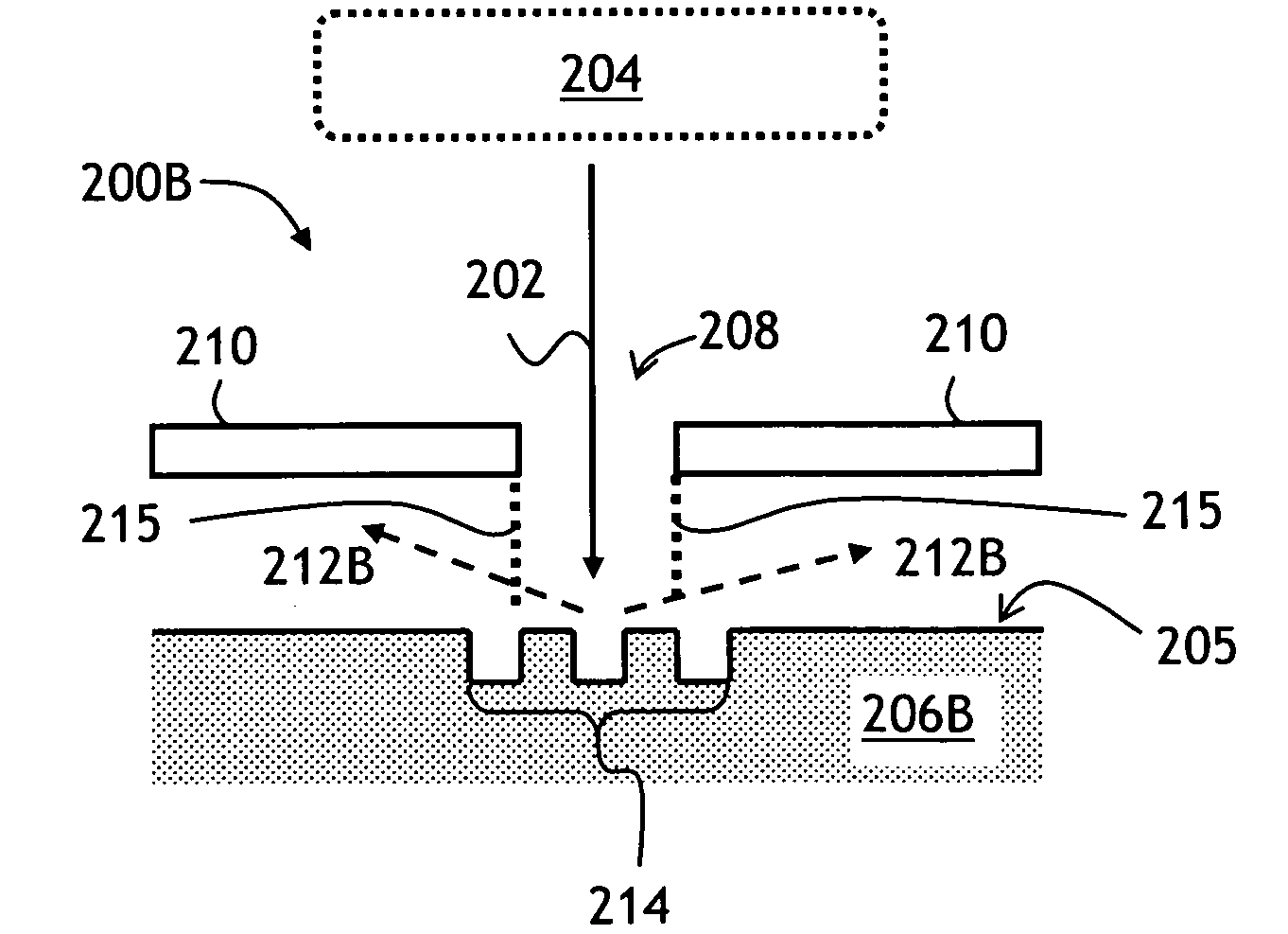
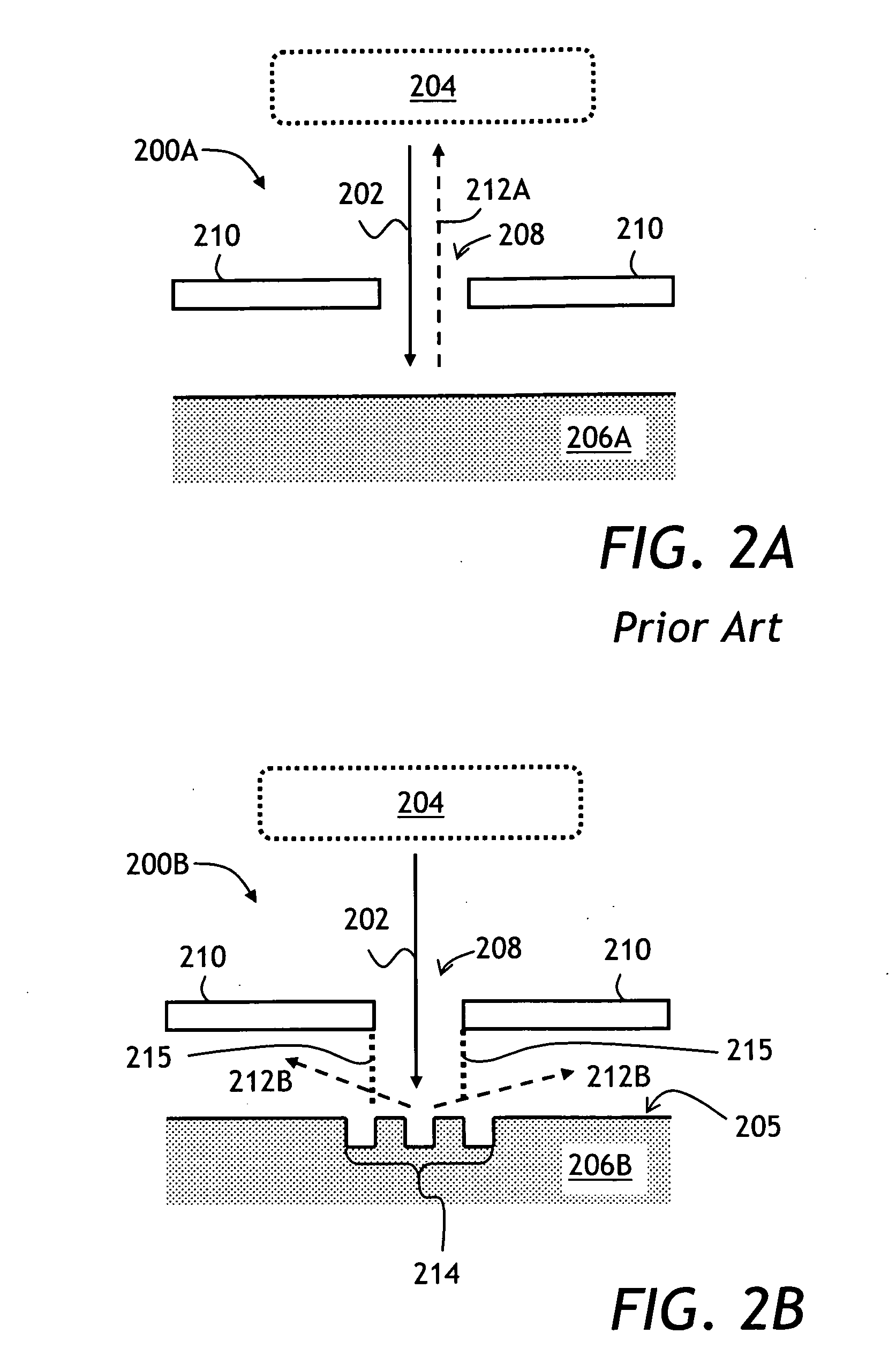
[0043]Referring to FIG. 2A, a problem solved by the present invention is illustrated by means of a cross-sectional view of a prior-art MEMS device 200A. In FIG. 2A, a light beam 202 from an optical system 204 reaches a MEMS substrate 206A through a gap 208 between the MEMS micromirrors 210 and is reflected back into the system 204 from the MEMS substrate 206A through the gap 208 as a beam 212A. Thus, an undesirable backreflection arises. The backreflected beam 212A degrades optical performance of the optical system 204.

[0044]To solve the problem, according to the present invention, a diffract...


PUM

PropertyMeasurementUnit
Fractionaaaaaaaaaa
Fractionaaaaaaaaaa
Fractionaaaaaaaaaa

Abstract

Diffractive patterns are disposed on a MEMS substrate in the gaps between the MEMS micromirrors to reduce backreflection of light leaking through the gaps and reflected by the MEMS substrate. The diffractive patterns are silicon surface-relief diffraction gratings or silicon oxide gratings on silicon substrate. Sub-wavelength gratings are used to suppress higher orders of diffraction; 50% duty cycle surface relief gratings on a substrate having index of refraction close to 3 are used to suppress both reflected and transmitted zero orders of diffraction simultaneously. The gratings have lines running parallel or at a slight angle to the gaps, to prevent the diffracted light from re-entering the gaps.

Description

CROSS-REFERENCE TO RELATED APPLICATIONS[0001]The present invention claims priority from U.S. provisional application No. 61 / 024,224, filed Jan. 29, 2008, which is incorporated herein by reference.TECHNICAL FIELD[0002]The present invention is related to micro-electro-mechanical systems (MEMS) micromirror devices, and in particular to improving optical performance of such devices.BACKGROUND OF THE INVENTION[0003]A micro-electromechanical system (MEMS) device is a micro-sized mechanical structure having electrical circuitry fabricated together with the device by using microfabrication processes mostly derived from integrated circuit fabrication processes. The developments in the field of MEMS process engineering allow for batch production of electrostatically tiltable MEMS micromirrors and micromirror arrays that can be used in such areas of photonics as visual displays, optical attenuators and switches, sensors with optical readout, and other devices. There are at least two main micro...

Claims


Application Information

Patent Timeline
IPC IPC(8): G02B26/00B32B37/14G02B5/18
CPCB32B38/10B32B38/145B32B2309/105Y10T156/10B32B2551/08G02B26/0808G02B26/0833B32B2457/00
Inventor MOIDU, ABDUL JALEEL K.COLBOURNE, PAULANDERSON, KEITHMILLER, JOHN MICHAEL
Owner LUMENTUM OPERATIONS LLC
Why Eureka
Try Eureka