Semiconductor light emitting device

Inactive Publication Date: 2009-08-06
HEAVY DUTY LIGHTING LLC
View PDF2 Cites 29 Cited by
  • Summary
  • Abstract
  • Description
  • Claims
  • Application Information

AI Technical Summary

Benefits of technology

[0008]An object of the present invention is to provide a semiconductor light emitting device exhibiting sufficient reliability in which the area of contact between the sealing resin for sealing and the metal member region having the light emitting elem...

Problems solved by technology

This also produces a problem that the lead electrodes cause an electrical short ...

Method used


Image

  • Semiconductor light emitting device
  • Semiconductor light emitting device
  • Semiconductor light emitting device

Examples


first embodiment

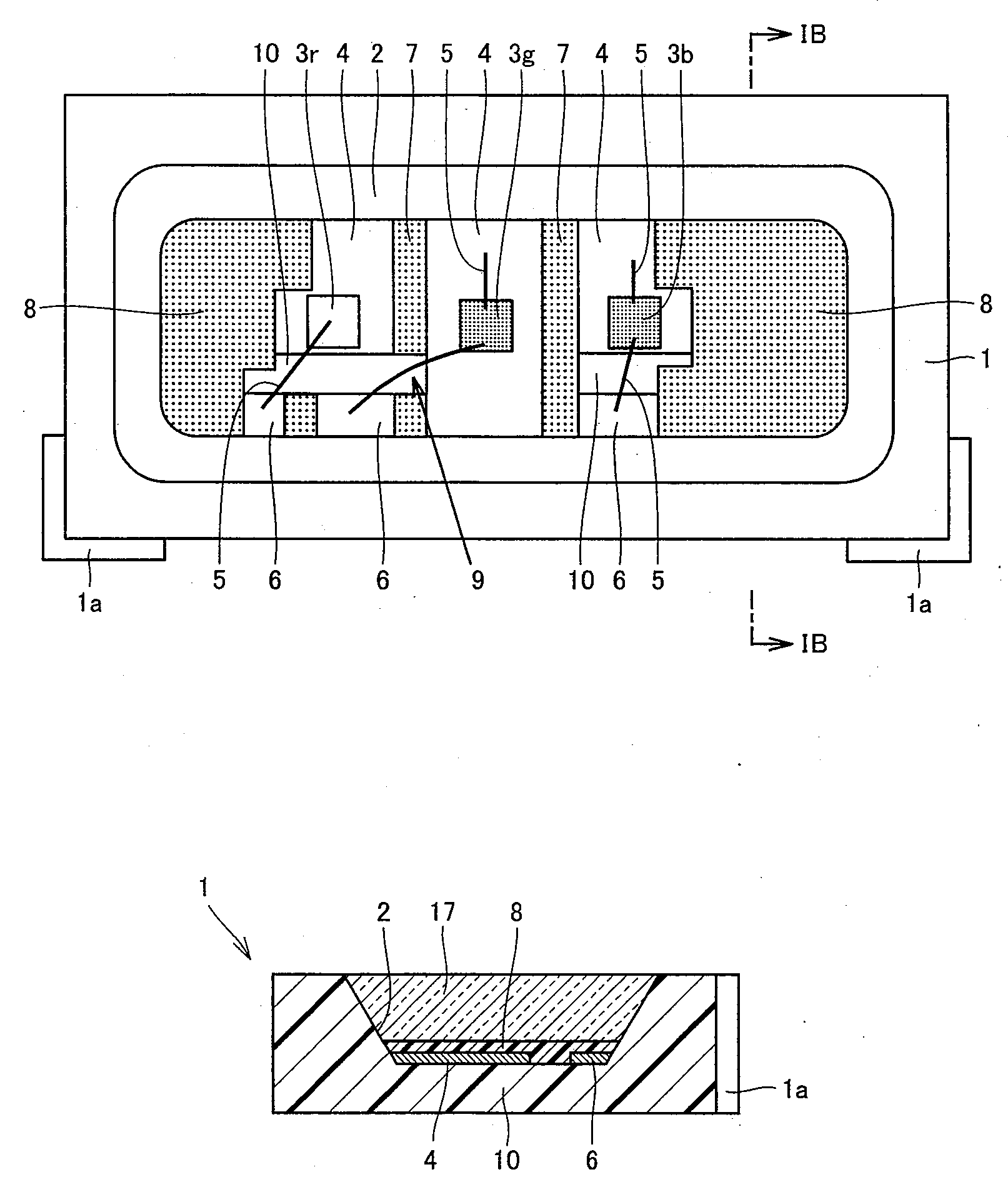
[0023]The semiconductor light emitting device according to the first embodiment of the present invention will be described with reference to FIGS. 1A and 1B. FIG. 1A is a diagram of a light emitting face corresponding to one side of a side-view type surface-mount light emitting diode as a semiconductor light emitting device according to the first embodiment of the present invention. FIG. 1B is a cross sectional view taken along lines IB-IB in FIG. 1A. FIGS. 1A and 1B each show a package 1 having a concave portion 2 formed on its light emitting face. Concave portion 2 forms an opening in which a light emitting element is placed, and the light emitting element is placed in this concave portion 2. The light emitting element includes a red light emitting element 3r, a blue light emitting element 3b and a green light emitting element 3g. These light emitting elements are arranged on the bottom surface of concave portion 2 in package 1 so as to be aligned in the longitudinal direction of ...

second embodiment

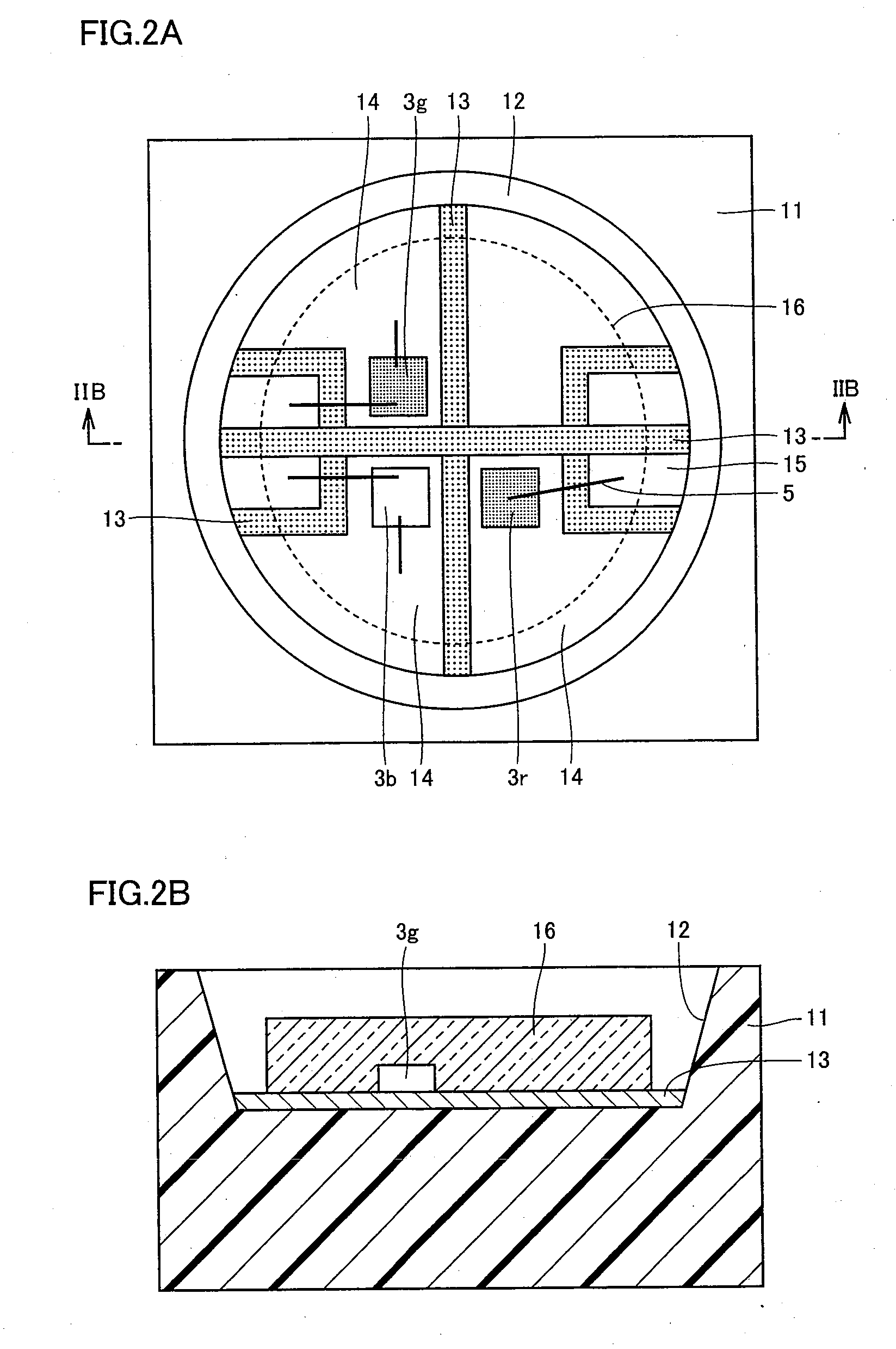
[0035]The semiconductor light emitting device according to the second embodiment of the present invention will be hereinafter described with reference to FIGS. 2A and 2B. FIG. 2A is a plan view of a top-view type surface-mount light emitting diode as a semiconductor light emitting device according to the second embodiment of the present invention, and FIG. 2B is a cross sectional view taken along lines IIB-IIB in FIG. 2A. With regard to the semiconductor light emitting device according to the second embodiment, the same components as those in the first embodiment are designated by the same reference characters, and description thereof will not be repeated. In FIG. 2A, a light emitting element (a red light emitting element 3r, a blue light emitting element 3b, a green light emitting element 3g), a convex resin portion 13, a conductive wire 5, an extraction electrode 14 as a metal member region, and an extraction electrode 15 are provided in a concave portion 12 of a package 11.

[0036]...

third embodiment

[0041]The semiconductor light emitting device according to the third embodiment of the present invention will be described with reference to FIG. 3. FIG. 3 is a plan view of a top-view type surface-mount light emitting diode including a zener diode as a semiconductor light emitting device according to the third embodiment of the present invention. With regard to the semiconductor light emitting device according to the third embodiment of the present invention, the same components as those in the first embodiment are designated by the same reference characters, and description thereof will not be repeated. In FIG. 3, in a concave portion 22 of a package 21, a blue light emitting element 3b, a convex resin portion 23, a conductive wire 5, an extraction electrode 24 as a metal member region, an extraction electrode 25, and a zener diode 26 are provided, which form a top-view type surface-mount light emitting diode.

[0042]When forming package 21, a silver-plated copper plate containing i...


PUM


Abstract

A silver-plated metal member region on which a light emitting element is disposed, an extraction electrode having a copper plate pattern, and a convex resin portion separating the metal member region into a plurality of sections are provided on the bottom surface of a concave portion in a package of a semiconductor light emitting device. A covering resin is partially formed on the metal member region and a sealing resin is placed to cover the metal member region, the covering resin and the convex resin portion. According to this configuration, the area of contact is decreased between the sealing resin and the metal member region having the light emitting element placed thereon, to thereby prevent the light emitting element from falling off and being displaced from the metal member region, with the result that a semiconductor light emitting device of high reliability can be provided.

Description

[0001]This nonprovisional application is based on Japanese Patent Application No. 2008-026694 filed on Feb. 6, 2008, with the Japan Patent Office, the entire contents of which are hereby incorporated by reference.BACKGROUND OF THE INVENTION[0002]1. Field of the Invention[0003]The present invention relates to a semiconductor light emitting device using a light emitting diode and the like.[0004]2. Description of the Background Art[0005]In the conventional surface-mount light emitting diode, as shown in FIG. 6, a plurality of light emitting elements 102 are arranged within a concave portion 101 of a package 100, and a plurality of lead electrodes 103 having light emitting elements 102 placed thereon, respectively, are arranged so as to be aligned in the longitudinal direction of package 100. A lead electrode 104 for wire bonding is disposed on the end of package 100 in the longitudinal direction located outside of lead electrode 103. Light emitting elements 102 are placed on different ...

Claims


Application Information

Patent Timeline
IPC IPC(8): H01L33/00H01L33/32H01L33/48H01L33/50H01L33/54H01L33/56H01L33/60H01L33/62
CPCH01L25/0753H01L33/54H01L2224/48247H01L2224/45144H01L2924/00H01L2224/48091H01L2224/48257H01L2924/00014
Inventor HATA, TOSHIOSHINOHARA, HISAYUKI
Owner HEAVY DUTY LIGHTING LLC
Why Eureka
Try Eureka