Sensor pixel and touch panel thereof

a touch panel and sensor technology, applied in the field of touch panel sensor pixel, can solve the problems of resistive touch panel not being able to determine the actual position of the pressure point, not all the equipments have common use input and output (i/o) interfaces for humans, resistive touch panel damage easily, etc., to save the volume of the touch panel and improve light transmission

Inactive Publication Date: 2009-08-13
HIMAX TECH LTD
View PDF6 Cites 33 Cited by
  • Summary
  • Abstract
  • Description
  • Claims
  • Application Information

AI Technical Summary

Benefits of technology

[0007]The invention provides a sensor pixel and a touch panel using the same that utilize a photo transistor to detect the situation of light obstruction on each sensor pixel, and thereby to indicate the location of the finger. Since the sensor pixel is the smallest detecting unit, the touch panel of the present invention not only can provide precise location of the finger or multi-finger, but also has no needs of disposing conductive layers for saving the volume of the touch panel and having better light transmission.
[0011]The present invention provides a sensor pixel and a touch panel using the same that utilize the characteristic of the photo transistor to detect the location of the finger or multi-finger. Since the photo transistor produces a photo leakage when it is exposed to a light, the present invention measures a voltage across the sensing capacitor and processes the voltage signal to judge whether the corresponding sensor pixel is touched. By proper timing control, the location of the finger or multi-finger can be immediately and precisely detected.

Problems solved by technology

Nevertheless, not all the equipments have common usage input and output (I / O) interfaces for human, such as keyboards or mice.
However, the resistive touch panel gets damaged easily by frequently pressing because of having no protective film, and only a single pressure point can be detected on the resistive touch panel.
If there is a plurality of pressure points, i.e. multi-finger, the resistive touch panel is not able to determine the actual position of the pressure point.
Besides, disposing the layers not only increases the thickness of the touch panel, but also affects the light transmission for liquid crystal display (LCD).
Furthermore, the resistive touch panels can not precisely locate the positions of the pressure points.
Consequently, the resistive touch panel cannot satisfy the requirement of consumers.
However, the optical touch panel is sensitive to even a tiny object or external light disturbance, and this matter causes incorrect position detection.
Therefore, the factories and stores extremely make effort on designing the touch panel that can solve the said problems and overcome the disadvantages.

Method used


Image

  • Sensor pixel and touch panel thereof
  • Sensor pixel and touch panel thereof
  • Sensor pixel and touch panel thereof

Examples


Embodiment Construction

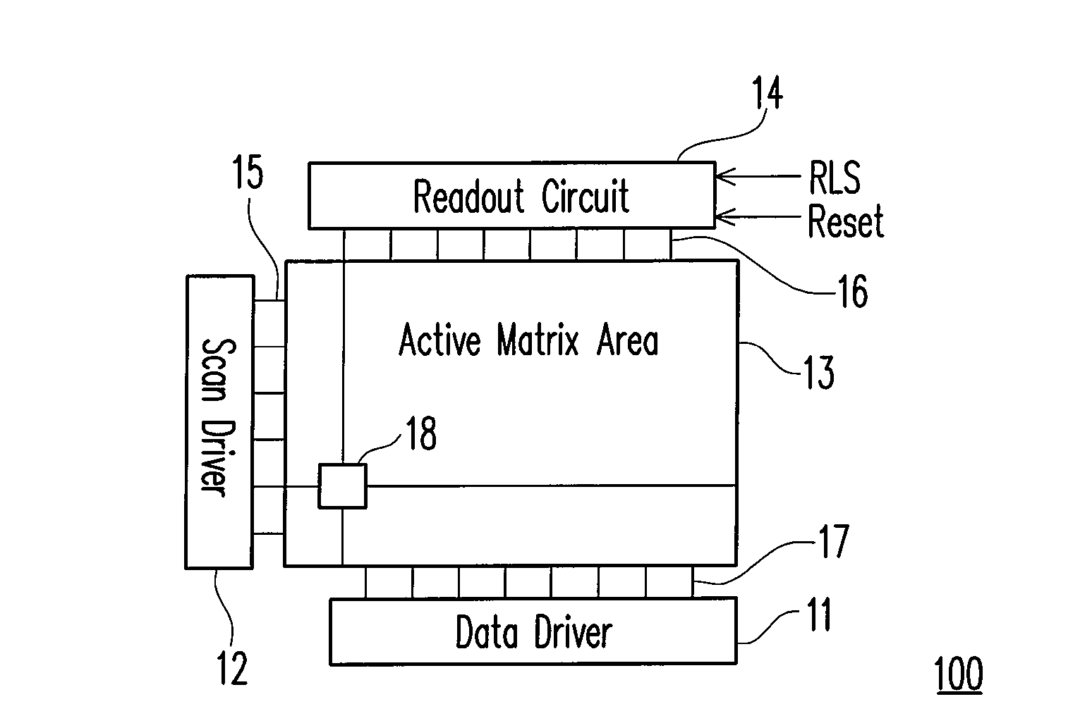
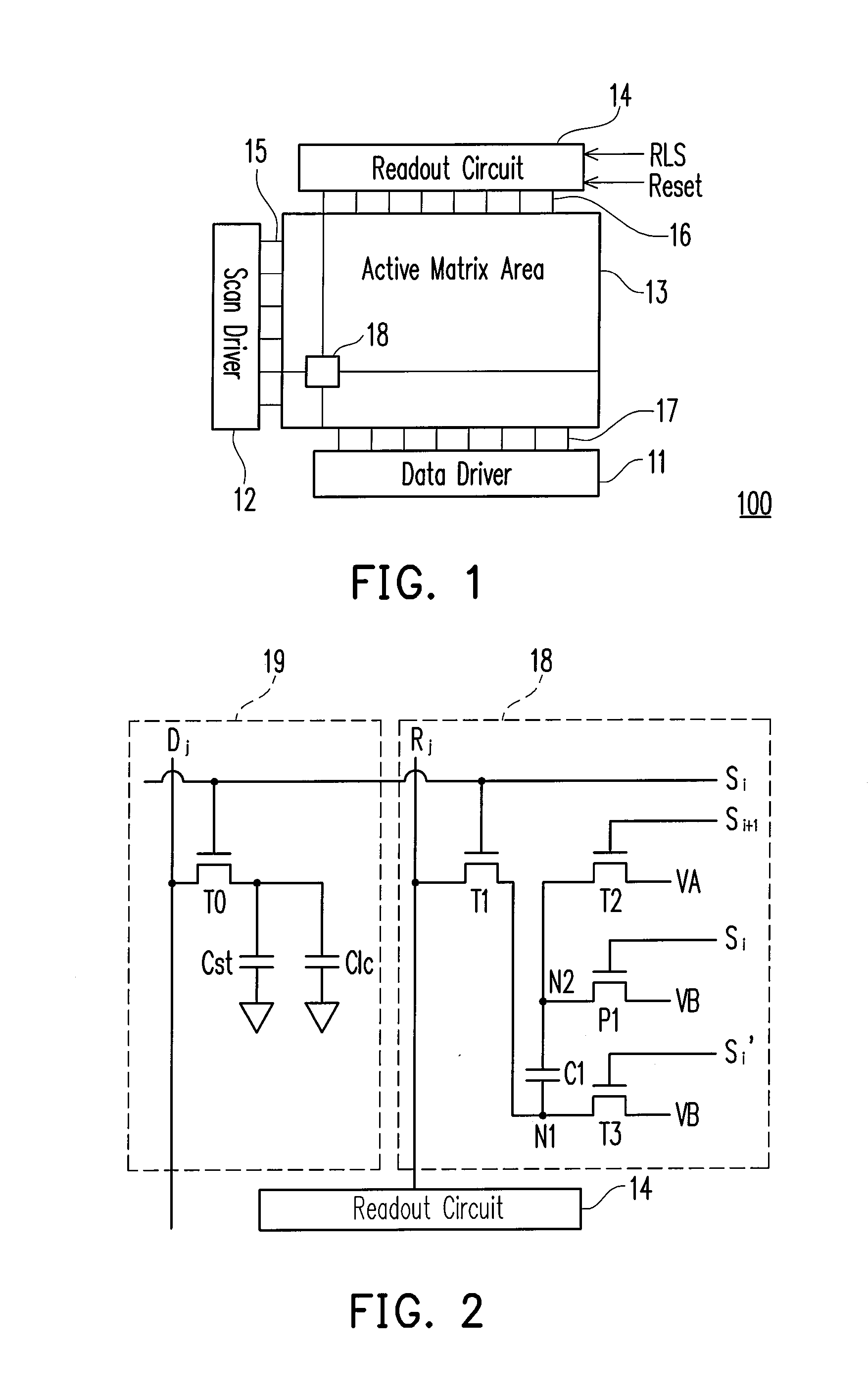
[0021]FIG. 1 is a diagram of the touch panel according to an embodiment of the present invention. Referring to FIG. 1, the touch panel 100 includes a scan driver 12, a data driver 11, a readout circuit 14 and an active matrix area 13, wherein the touch panel 100 has m scan lines 15 and n readout lines 16. There are a plurality of display pixels (not illustrated in FIG. 1) and a plurality of sensor pixels 18 arranged in the active matrix area 13. The scan driver 12 transmits a scan driving signal to the display pixels through the scan lines 15 and the data driver 11 transmits a data driving signal to the display pixels through the data lines 17 for displaying an image frame.

[0022]FIG. 2 is a circuit diagram of the display pixel and the sensor pixel coupled together according to the embodiment of the present invention. Referring to FIG. 2, the display pixel 19 includes a transistor T0, a storage capacitor Cst and a liquid crystal layer, represented by a capacitor Clc. The transistor T...


PUM


Abstract

A sensor pixel and a touch panel using the same are provided herein, wherein the touch panel has m scan lines and n readout lines. The sensor pixel includes a sensing capacitor, a readout transistor, a reset transistor, a base transistor, and a photo transistor. The photo transistor included in the sensor pixel produces a photo leakage current when it is exposed to a light. The light obstruction characteristic of the photo transistor is utilized to detect the locations of the touched sensor pixels. By proper timing control, the present invention not only can be applied to the multi-finger detection, but also is easy to be implemented.

Description

BACKGROUND OF THE INVENTION[0001]1. Field of Invention[0002]The present invention relates to a sensor pixel of a touch panel, and more particular, utilizes the sensor pixel having a photo transistor to detect a location of the finger.[0003]2. Description of the Related Art[0004]With great advance of electronic technique and popularity of wireless communication and internet, the portable devices having light, thin and small advantages gradually become a data access platform in a new generation. Nevertheless, not all the equipments have common usage input and output (I / O) interfaces for human, such as keyboards or mice. Hence, the touch panel is often applied to be a human-machine interface between human and intelligent equipments for controlling.[0005]Generally, the resistive touch panel is composed of two conductive layers separated by thin space. When users press the touch panel, the layers are connected at certain point and thereby a voltage variation corresponding to the certain ...

Claims


Application Information

Patent Timeline
Patent Type & Authority Applications(United States)
IPC IPC(8): G06F3/041
CPCG06F3/042G06F3/0412
Inventor CHUANG, KAI-LAN
Owner HIMAX TECH LTD
Why Eureka
Try Eureka