

Substrate processing method and apparatus, method for manufacturing semiconductor device and storage medium
a processing method and semiconductor technology, applied in the direction of cleaning using liquids, other chemical processes, semiconductor/solid-state device details, etc., can solve the problems of deterioration of semiconductor devices, damage to interlayer insulating films, and easy oxidation of cu,
- Summary
- Abstract
- Description
- Claims
- Application Information
AI Technical Summary
Benefits of technology
Problems solved by technology
Method used
Image

Examples
first embodiment
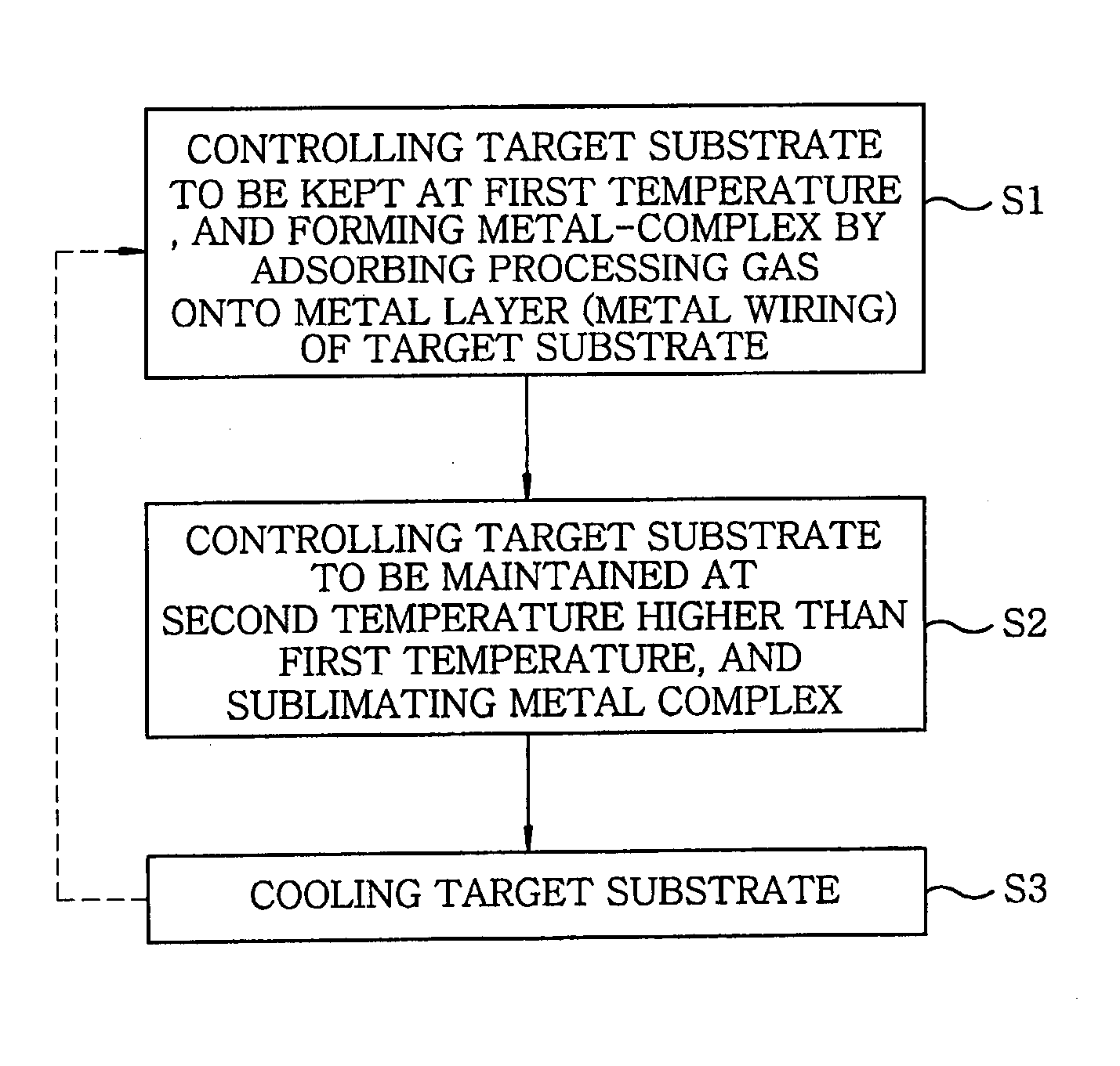
[0052]FIG. 1 is a flowchart for describing a substrate processing method in accordance with a first embodiment of the present invention.
[0053]Referring to FIG. 1, in a step 1 (in the drawing, it is defined as a step S1, and the other following steps will be numbered likewise), a target substrate, which has a metal layer (e.g., a metal wiring or the like) whose surface is oxidized and thus provided with a metal oxide film, is disposed in a processing space inside a processing vessel, and the target substrate is controlled (set) to be kept at a first temperature. Here, an organic compound gas such as formic acid or the like is introduced into the processing vessel (processing space) to be adsorbed in the surface of the metal layer on the target substrate, thereby obtaining a metal-complex (metal-organic compound complex).
[0054]To suppress sublimation of the metal-organic compound complex formed in the step 1, it is preferable to set the temperature of the target substrate to be at a l...
second embodiment
[0161]A Cu oxide film is removed by performing a substrate processing in accordance with the above-described substrate processing method and an analysis on the removal result is explained hereinafter. Here, a specific example of removing the Cu oxide film for the first time will be described.
[0162]First, vaporized formic acid (processing gas) was supplied to a target substrate having Cu whose surface had been oxidized. The formic acid was adsorbed in the surface of the Cu, so that a metal complex (metal-organic compound complex) was formed. The adsorption of the formic acid was checked by a degas analysis of the target substrate. In this example, the internal pressure of a processing space accommodating the target substrate therein was set to be maintained within a range from about 0.4 to 0.7 kPa, and the temperature of the target substrate was maintained substantially at a room temperature (step 1).
[0163]Then, the target substrate was heated in a processing space maintained in a de...
third embodiment
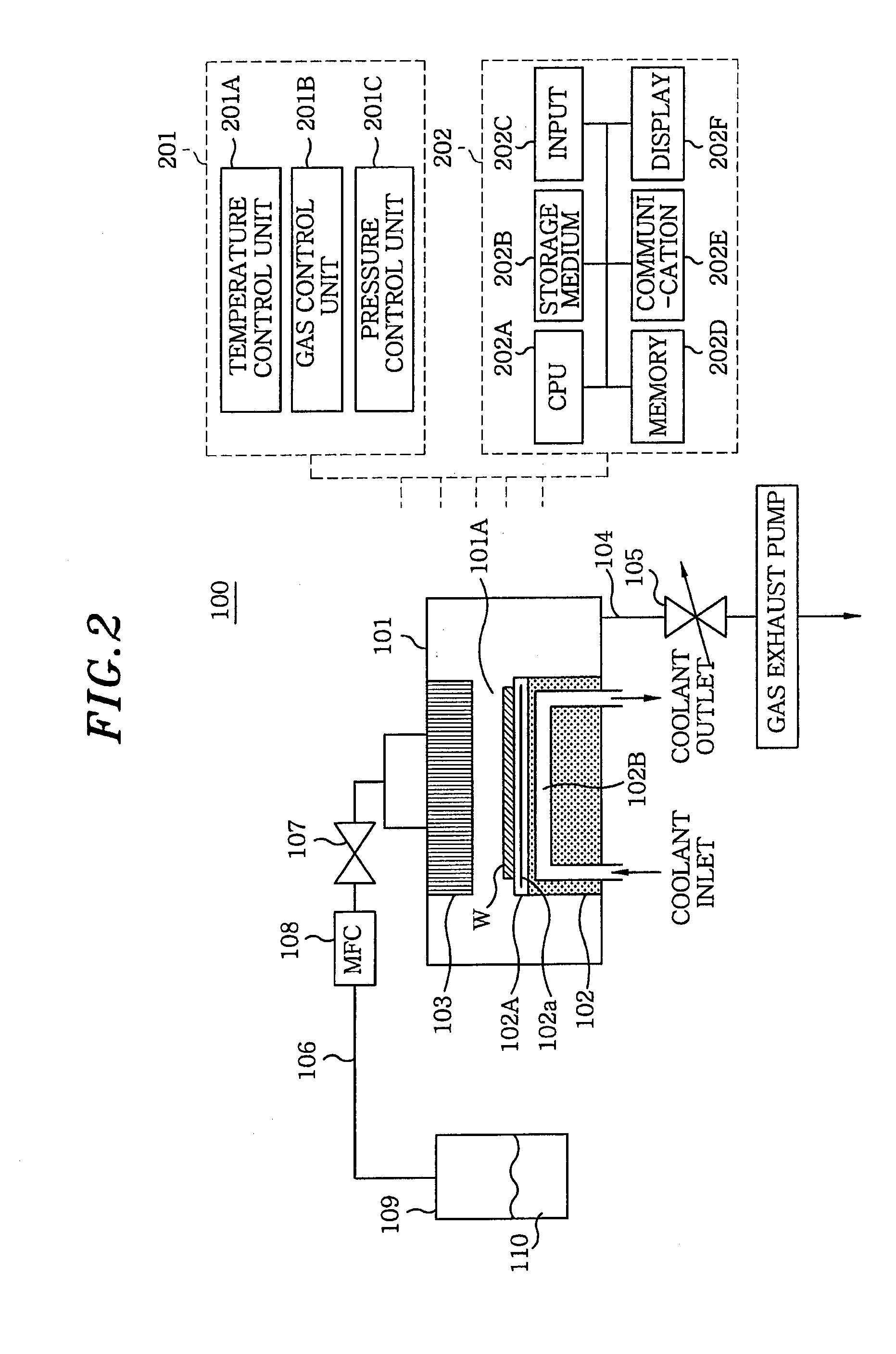
[0172]Hereinafter, an example of the processing unit 100D, which is a processing unit (substrate processing apparatus) capable of performing the conventional substrate processing method (i.e., the method of performing the formation and the sublimation of the metal-organic compound complex together) and capable of removing metal deposits attached to the inside thereof, will be explained with reference to FIG. 13. Like the processing chamber 100 (100A to 100C) described earlier, the processing chamber 100D functions as a part of the cluster substrate processing apparatus and is used by being connected to the transfer chamber 301, for example.
[0173]As shown in FIG. 13, the processing unit 100D includes a processing vessel 131 having a processing space 131A therein, and a supporting table 132 for sustaining a target substrate W thereon is installed in the processing space 131A.
[0174]A heating unit 132A made up of, e.g., a heater is embedded in the supporting table 132. The target substr...
PUM
| Property | Measurement | Unit |
|---|---|---|
| temperature | aaaaa | aaaaa |
| temperature | aaaaa | aaaaa |
| pressure | aaaaa | aaaaa |
Abstract
Description
Claims
Application Information