Quad flat non-leaded package structure

a non-leaded, flat technology, applied in the direction of semiconductor devices, semiconductor/solid-state device details, electrical apparatus, etc., to achieve the effect of prolonging the life of the package, avoiding damage to the cutting tool, and improving the reliability of the bonding process

Inactive Publication Date: 2009-08-20
CHIPMOS TECH INC
View PDF12 Cites 10 Cited by
  • Summary
  • Abstract
  • Description
  • Claims
  • Application Information

AI Technical Summary

Benefits of technology

[0010]Accordingly, the present invention is directed to a QFN package structure, which may improve reliability

Problems solved by technology

Moreover, the molding compound encapsulates the chip, a portion o

Method used


Image

  • Quad flat non-leaded package structure
  • Quad flat non-leaded package structure
  • Quad flat non-leaded package structure

Examples


Embodiment Construction

[0030]In the following content, a plurality of package structures are taken as examples for describing the present invention, though these examples are not used for limiting the present invention.

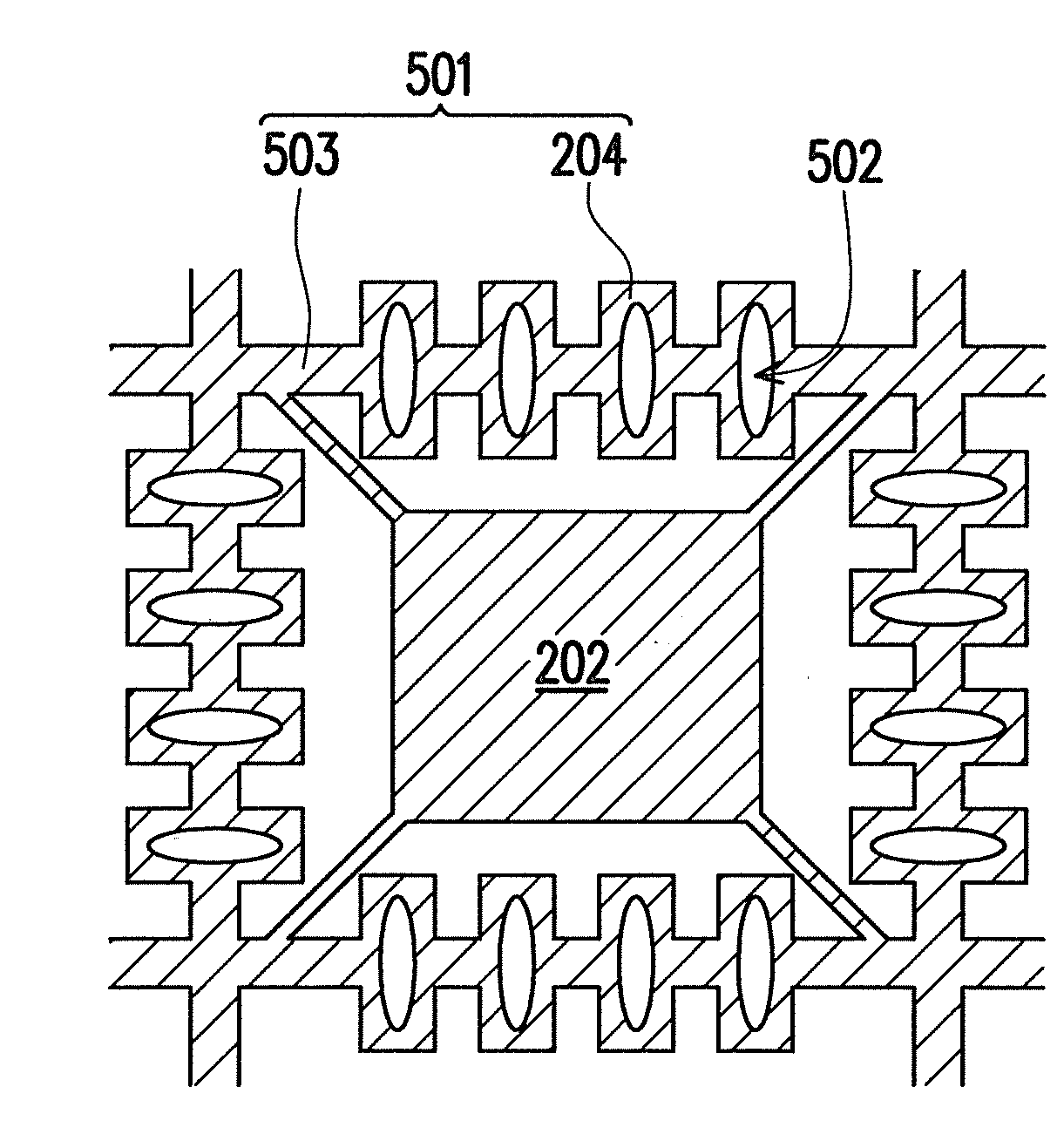
[0031]FIG. 2A is a cross-sectional view of a QFN package structure according to an embodiment of the present invention. FIG. 2B is bottom view of the QFN package structure of FIG. 2A.

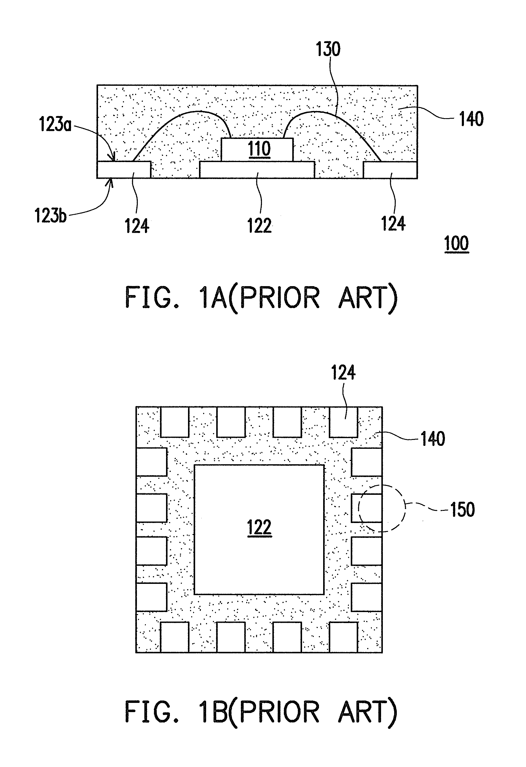
[0032]Referring to FIG. 2A and FIG. 2B, the package structure includes a die pad 202, a plurality of leads 204, a chip 206 and a molding compound 208. The die pad 202 has a top surface 201a and an opposite bottom surface 201b, and the leads 204 are disposed around the die pad 202. Material of the die pad 202 and the leads 204 can be metal materials such as copper, copper alloy or nickel-iron alloy.

[0033]A plurality of bonding pads 210 can be disposed on the chip 206, and the chip 206 is disposed on the top surface 201a of the die pad 202. In an embodiment, an adhesive layer 212 can be disposed between the chip ...


PUM


Abstract

A quad flat non-leaded package structure including a die pad, a plurality of leads, a chip, and a molding compound is provided. The die pad has a top surface and an opposite bottom surface, and the leads are disposed around the die pad. A concave portion is disposed at the end of each leads. The chip is disposed on the top surface of the die pad and is electrically connected to the leads. The molding compound encapsulates the chip, a portion of the leads and the die pad, and fills the gaps between the leads.

Description

CROSS-REFERENCE TO RELATED APPLICATION[0001]This application claims the priority benefit of Taiwan application serial no. 97105927, filed on Feb. 20, 2008. The entirety of the above-mentioned patent application is hereby incorporated by reference herein and made a part of specification.BACKGROUND OF THE INVENTION[0002]1. Field of the Invention[0003]The present invention relates to a chip package structure. More particularly, the present invention relates to a quad flat non-leaded (QFN) package structure.[0004]2. Description of Related Art[0005]In the semiconductor industry, the fabrication of integrated circuits (IC) can be divided into three phases: IC design, IC fabrication process, and IC packaging.[0006]Regarding IC packaging, a chip is fabricated through wafer fabrication, circuit design, photolithography and etching processes, and wafer dicing, etc. Each chip is electrically connected to a substrate through a bonding pad on the chip, and the chip is encapsulated by a molding c...

Claims


Application Information

Patent Timeline
IPC IPC(8): H01L23/495
CPCH01L23/3107H01L23/49541H01L23/49548H01L29/0657H01L24/48H01L2224/48247H01L2924/01079H01L2224/48091H01L2924/00014H01L2924/14H01L2924/181H01L2224/45144H01L24/45H01L2924/00H01L2924/00012H01L2224/45015H01L2924/207
Inventor WU, CHENG-TING
Owner CHIPMOS TECH INC
Why Eureka
Try Eureka