Liquid crystal display device

a display device and liquid crystal technology, applied in static indicating devices, non-linear optics, instruments, etc., can solve the problem of high manufacturing cost, and achieve the effect of simplifying fabrication and assembly operation, and reducing manufacturing cos

Active Publication Date: 2009-08-20
PANASONIC LIQUID CRYSTAL DISPLAY CO LTD +1
View PDF4 Cites 20 Cited by
  • Summary
  • Abstract
  • Description
  • Claims
  • Application Information

AI Technical Summary

Benefits of technology

[0010]Accordingly, the invention has been made to solve the above-described conventional problem, and it is an object of the invention to provide a liquid crystal display device which can reduce the manufacturing cost by reducing the number of parts and simplifying the fabrication and the assembling operation, for the conduction between a conductive frame and a color filter substrate.

Problems solved by technology

However, since the thus configured liquid crystal display device uses the conductive tape or conductive paste for the conduction between the conductive frame and the color filter substrate, the number of constituent members and the number of mounting steps (operations) therefor increase, resulting in a problem that the manufacturing cost is high.

Method used


Image

  • Liquid crystal display device
  • Liquid crystal display device
  • Liquid crystal display device

Examples


embodiment 1

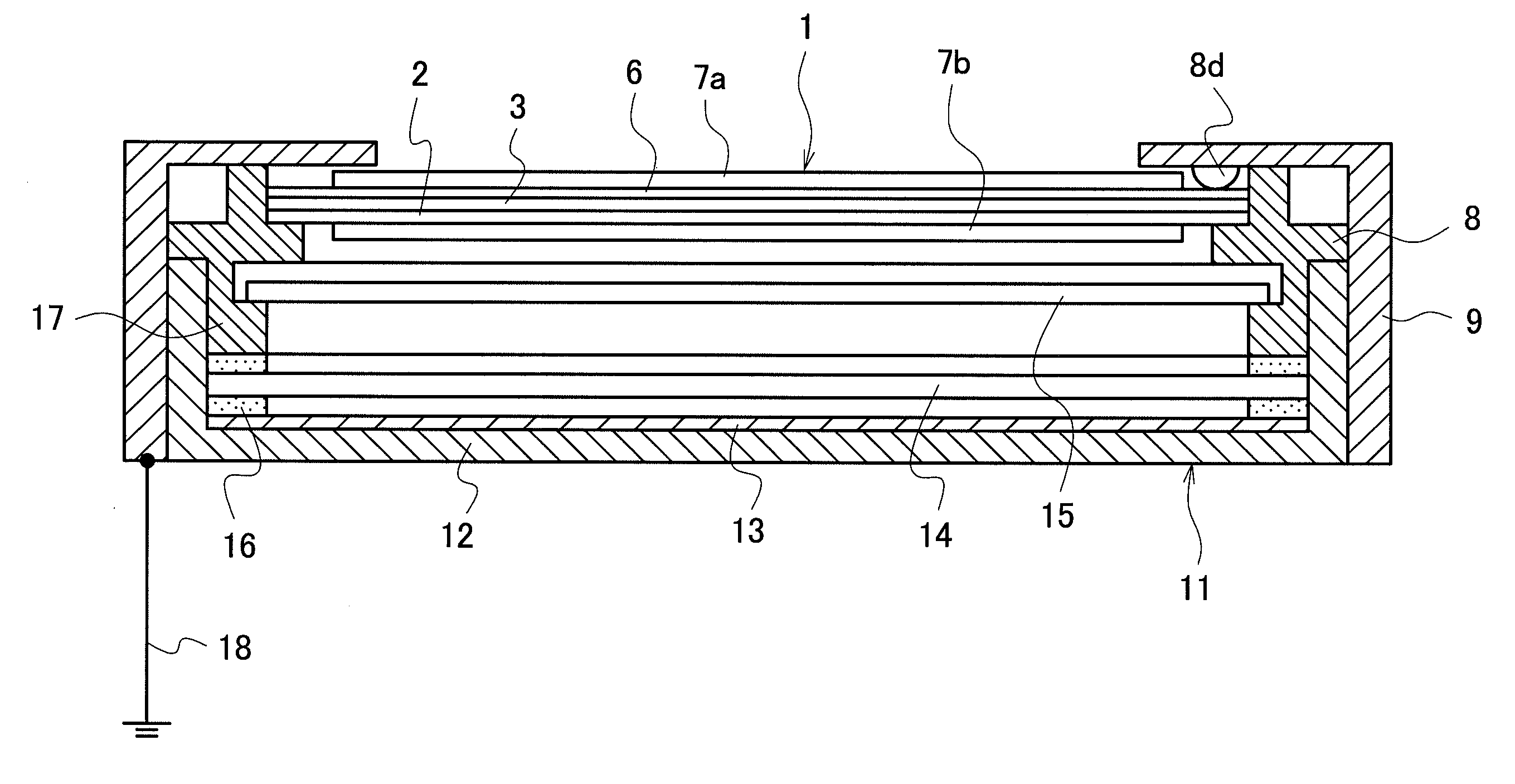
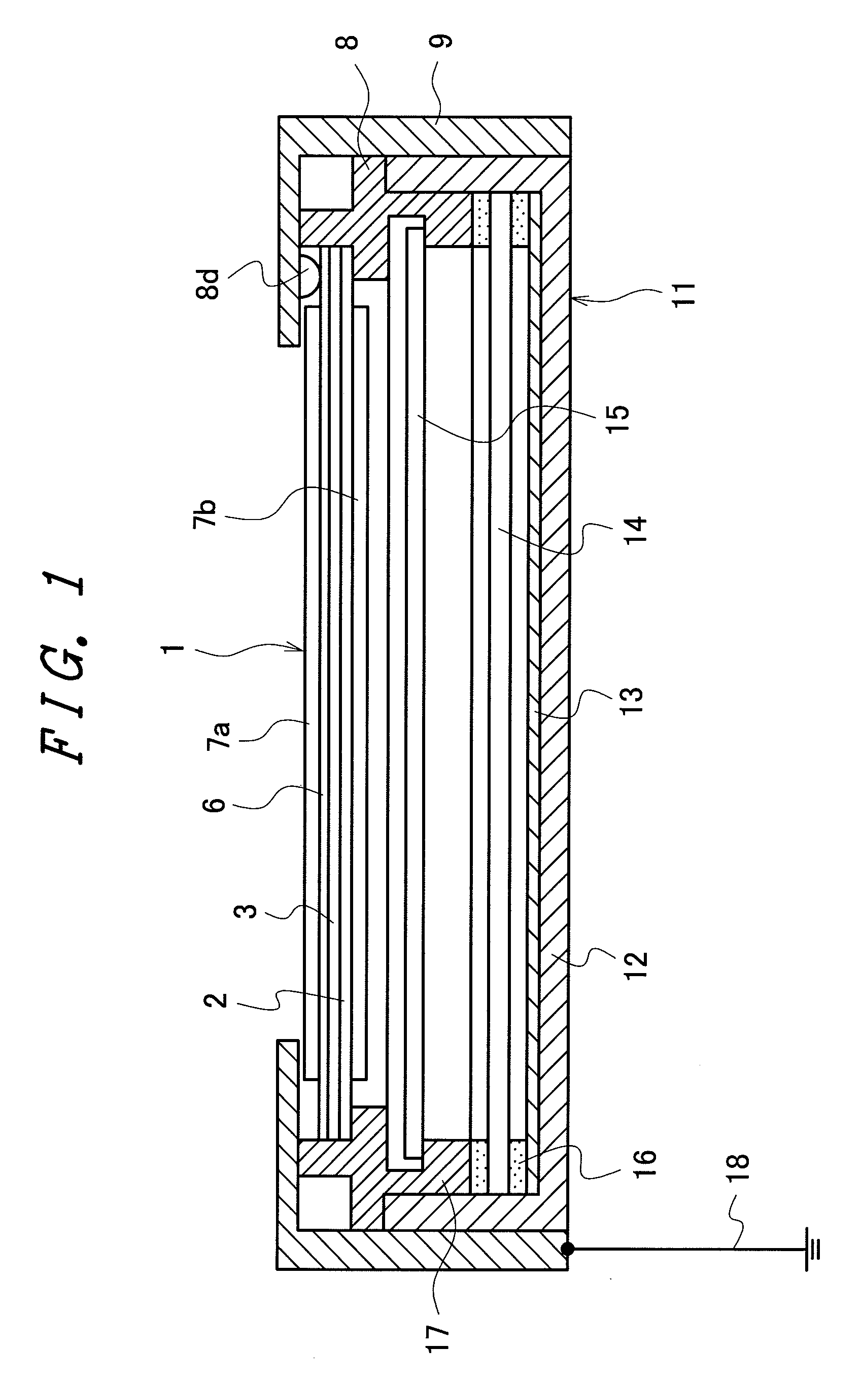
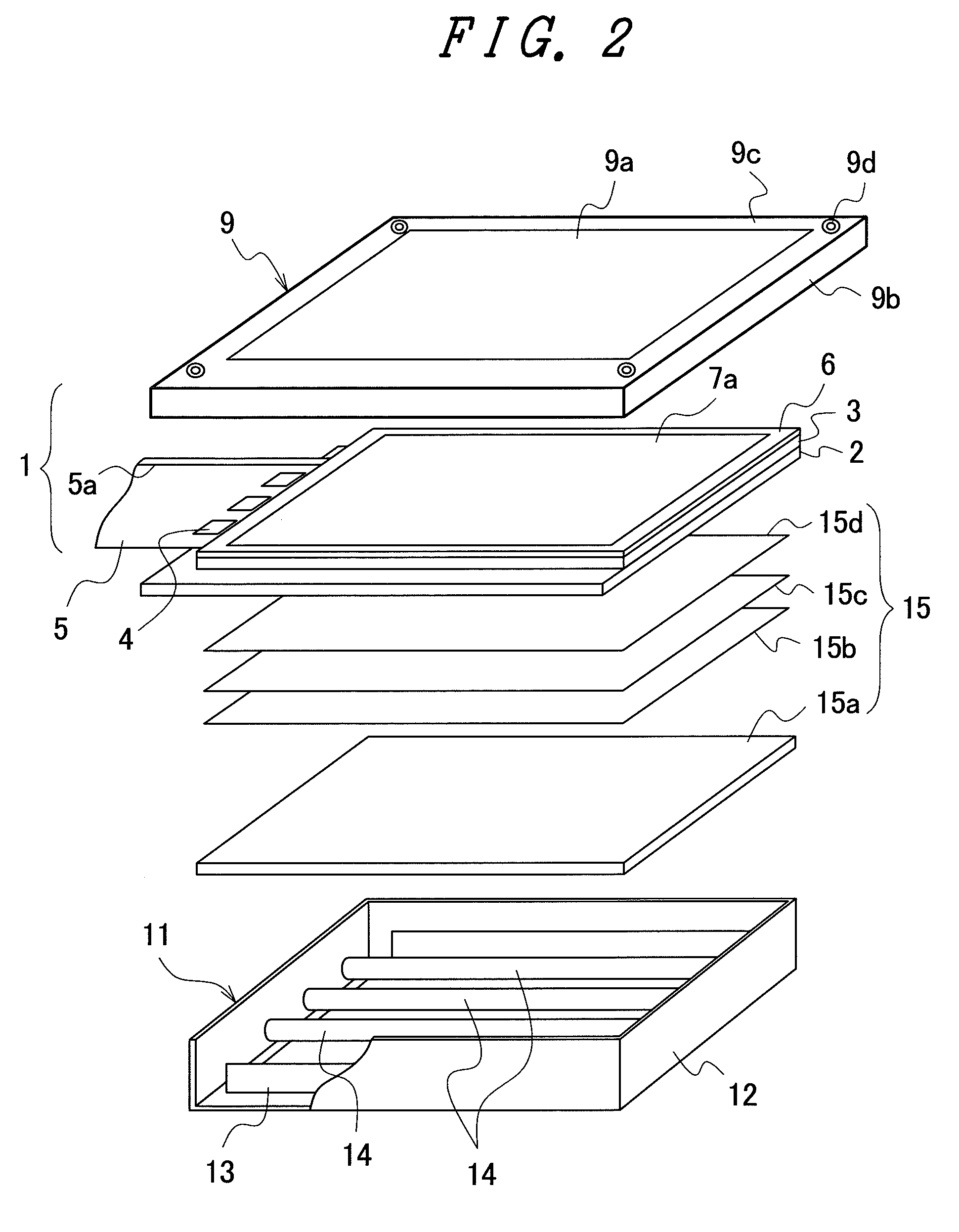
[0032]FIG. 1 is a principal part schematic cross-sectional view for explaining a configuration of an embodiment of a liquid crystal display device according to the invention, while FIG. 2 is a principal part schematic development perspective view of FIG. 1.

[0033]In FIGS. 1 and 2, a liquid crystal display panel 1 of the horizontal electric field type has a liquid crystal layer sealed between two translucent glass substrates each having an electrode for forming pixel (not shown). One side of one glass substrate (generally referred to as an “active matrix substrate” or “thin film transistor substrate”) 2 which is a first substrate formed with a thin film transistor, a pixel electrode, and the like extends off the other glass substrate (generally referred to as a “color filter substrate”) 3 which is a second substrate formed with a color filter. An electrode terminal part is formed on the portion which extends off the glass substrate 3, and a flexible printed circuit board 5 on which ch...

embodiment 2

[0047]FIGS. 4A and 4B are a principal part plan view and a cross-sectional view, respectively, of a panel frame for explaining another embodiment of the liquid crystal display device according to the invention, in which the same reference numerals are assigned to the same parts as those in the above-described drawings, and the explanations thereof will be omitted. FIGS. 4A and 4B differ from FIGS. 3A and 3B in that each of slit parts 9f extending in a screen center direction is formed on the upper surface part 9c of the panel frame 9 formed to have a rectangular shape at a corner part formed by one side of the rectangle and another side adjacent to the one side. Further, the panel frame of Embodiment 2 is formed with protruding parts 9g each covering the periphery part of the liquid crystal display panel 1 from the front surface side and drawn in a curved shape toward a front surface direction of the liquid crystal display panel 1. The protruding part 9g is formed on the entire area...


PUM


Abstract

The invention provides a liquid crystal display device which can reduce the manufacturing cost by reducing the number of parts and simplifying the fabrication and the assembling operation, for the conduction between a metal frame and a color filter substrate. A liquid crystal display panel has a conductive layer on a front surface of a second glass substrate. A panel frame has a side wall part extending along a side wall of the liquid crystal display panel and an upper surface part extending from the side wall part toward a front surface direction of the liquid crystal display panel, integrally formed together. The upper surface part is in contact with the conductive layer of the liquid crystal display panel. A constant potential is applied to the panel frame.

Description

CROSS-REFERENCE TO RELATED APPLICATION[0001]The present application claims priority from Japanese application JP2008-32670 filed on Feb. 14, 2007, the content of which is hereby incorporated by reference into this application.BACKGROUND OF THE INVENTION[0002]1. Field of the Invention[0003]The present invention relates to a liquid crystal display device, particularly, to a liquid crystal display device of a horizontal electric field type so-called IPS (In-Plane Switching) type, and more specifically to an antistatic structure for a liquid crystal display panel housed in a panel frame.[0004]2. Description of Related Art[0005]Active matrix type liquid crystal display devices which use an active element represented by a thin film transistor (TFT) come in to widespread use as various display devices because of features that they are thin and light in weight and in view of high image quality. The display type of the liquid crystal display device is mainly classified into the following two...

Claims


Application Information

Patent Timeline
Patent Type & Authority Applications(United States)
IPC IPC(8): G09G3/36
CPCG02F1/134363G02F1/133308
Inventor ARISATO, KOZOICHIO, MASAKI
Owner PANASONIC LIQUID CRYSTAL DISPLAY CO LTD
Why Eureka
Try Eureka