Artificial optic nerve network module, artificial retina chip module, and method for fabricating the same

an optic nerve network module and chip module technology, applied in intraocular lenses, medical science, therapy, etc., can solve the problems of insufficient matching of i/o increments, inability to real-time transmit, and lower transmission rate, so as to reduce the risk of retina injury and insufficient flexibility of conventional artificial retinas

Inactive Publication Date: 2009-08-20
IND TECH RES INST
View PDF13 Cites 8 Cited by
  • Summary
  • Abstract
  • Description
  • Claims
  • Application Information

AI Technical Summary

Benefits of technology

[0010]Accordingly, the present invention is directed to an artificial optic nerve network module. The artificial optic nerve network module uses biocompatible and flexible polymer bumps serving as electrical contacts for connecting different chips to replace the conventional metal electrodes. This arrangement may avoid the injuries to the retina caused by the rigid metal electrodes having no elasticity when the eyeball turns suddenly.
[0017]The present invention forms a plurality of flexible polymer bumps on the chip by the using steps of drilling holes, forming a conductive layer, coating and patterning a polymer layer, etc. In such a way, the present invention utilizes the polymer bumps serving as electrical contacts instead of the conventional technology which using the wire bonding technique for electrically connecting the photodiode plate and the signal processing chip. This manner may solve the problem that the wire bonding technique cannot be applied to chips having a large I / O number and achieve real-time transmission.
[0018]Besides, the present invention employs a three-dimensional chip stack technology with the flexible polymer bumps made of the biocompatible polymer material to connect the signal processing chip and the photodiode array chip for miniaturization. This may provide a solution to the insufficient flexibility of the conventional artificial retinas and the risk of injuries to the retina caused by the rigid metal electrodes when the eyeball turns suddenly.

Problems solved by technology

However, as the amount of the electrode arrays (pixels) increasing, the conventional wire bonding technique is not sufficient for matching the increment of the I / O number.
Further, the signal transmittance by using the wire bonding technique for electrical connection may encounter the problems of a lower transmission rate and incapable of real-time transmission.

Method used


Image

  • Artificial optic nerve network module, artificial retina chip module, and method for fabricating the same
  • Artificial optic nerve network module, artificial retina chip module, and method for fabricating the same
  • Artificial optic nerve network module, artificial retina chip module, and method for fabricating the same

Examples


Embodiment Construction

[0025]Reference will now be made in detail to the present preferred embodiments of the invention, examples of which are illustrated in the accompanying drawings. Wherever possible, the same reference numbers are used in the drawings and the description to refer to the same or like parts.

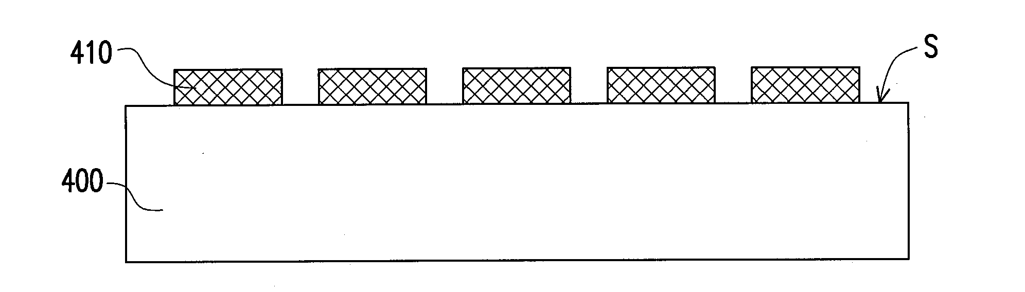
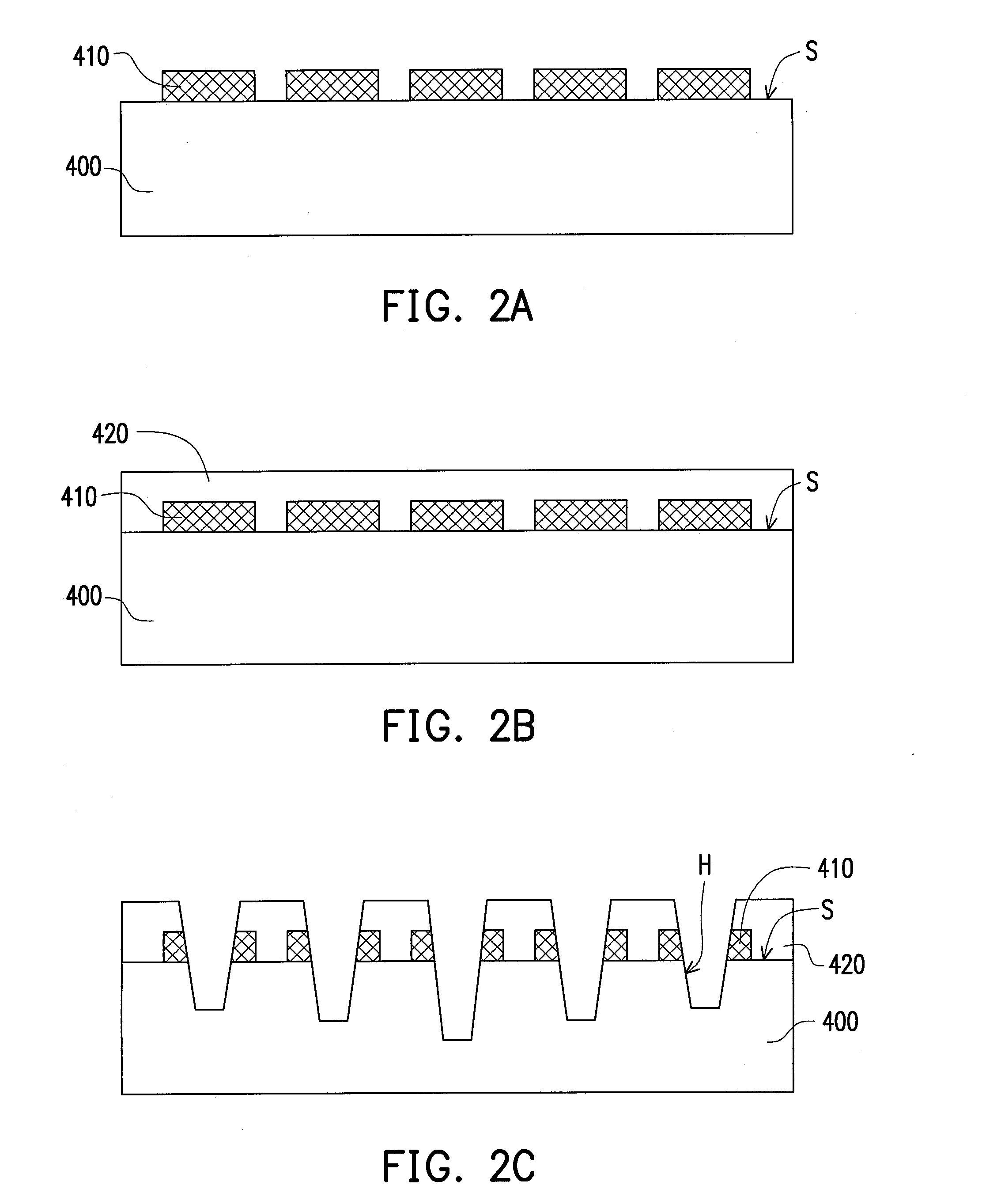
[0026]FIGS. 2A through 2J are schematic, cross-sectional diagrams illustrating the process flow for fabricating an artificial retina chip module according to an embodiment of the present invention. First, please refer to FIG. 2A, a signal processing chip 400 is provided for converting a light signal into an electronic signal, and outputting a suitable signal for stimulating optic nerves. The signal processing chip 400 includes a plurality of pads 410 disposed on a surface S thereof. As shown in FIG. 2B, a photo resist layer 420 is formed on the surface S of the signal processing chip 400 for covering the pads 410.

[0027]Then, as shown in FIG. 2C, a plurality of micro holes H is formed. Each of the mic...


PUM


Abstract

An artificial retina chip module including a signal processing chip, a first polymer bump layer, and a photodiode array chip is provided. The signal processing chip includes a plurality of first pad disposed on a surface thereof. The first polymer bump layer includes a plurality of polymer bumps insulated from one another. Each of the first polymer bumps is composed of a polymer material and a conductive layer coated on the polymer material. Each first polymer bump is embedded into the corresponding first pad and the signal processing chip, wherein one end of the first polymer bump protrudes from the first pad and the other end thereof protrudes from a back surface of the signal processing chip. The photodiode array chip is disposed at one side of the signal processing chip and is electrically connected to the signal processing chip through the first polymer bumps.

Description

CROSS-REFERENCE TO RELATED APPLICATION[0001]This application claims the priority benefit of Taiwan application serial no. 97105776, filed on Feb. 19, 2008. The entirety of the above-mentioned patent application is hereby incorporated by reference herein and made a part of specification.BACKGROUND OF THE INVENTION[0002]1. Field of the Invention[0003]The present invention generally relates to an artificial optic nerve network module, an artificial retina chip module and a method for fabricating the same, and more particularly, to an artificial optic nerve network module and an artificial retina chip module which utilize flip chip bonding technique for electrical connecting different chips, and a method for fabricating the same.[0004]2. Description of Related Art[0005]In the past, ophthalmology could do little about diseases related to retina pathological changes, such as macular degeneration, and retinitis pigmentosa (RP). Conventional technologies are used to strengthen remaining vis...

Claims


Application Information

Patent Timeline
Patent Type & Authority Applications(United States)
IPC IPC(8): A61F2/14
CPCA61F2/141A61N1/36046A61F9/08
Inventor CHANG, TAO-CHIHLEE, MIN-LIN
Owner IND TECH RES INST
Why Eureka
Try Eureka