Scanning electron microscope and method of measuring pattern dimension using the same

Inactive Publication Date: 2009-08-27
HITACHI HIGH-TECH CORP
View PDF2 Cites 13 Cited by
  • Summary
  • Abstract
  • Description
  • Claims
  • Application Information

AI Technical Summary

Benefits of technology

[0011]The present invention relates to conducting high-precision dimensional measurement which is little aff

Problems solved by technology

However, the above method had weak points in that the it was difficult to know exactly to which part of the cross-section the measured dimension corresponded (for example, whether the top portion of the pattern or the bottom portion).
Another problem was that when the cross-sectional shape of the pattern changed, measuring errors could also occur depending on the shape.
With the advancement of microfabrication in the semiconductor manufacturing process, such variation in measuring error has an unignorable effect, and therefore, it is necessary to resolve such error for the purpose of realizing high-pr

Method used


Image

  • Scanning electron microscope and method of measuring pattern dimension using the same
  • Scanning electron microscope and method of measuring pattern dimension using the same
  • Scanning electron microscope and method of measuring pattern dimension using the same

Examples


Embodiment Construction

[0032]Hereafter, explanation is made of the preferred embodiments based on the drawings. Additionally, in the drawings to explain about the preferred embodiments, the members having the same function are marked with the same numerals, with repetition of explanation being omitted.

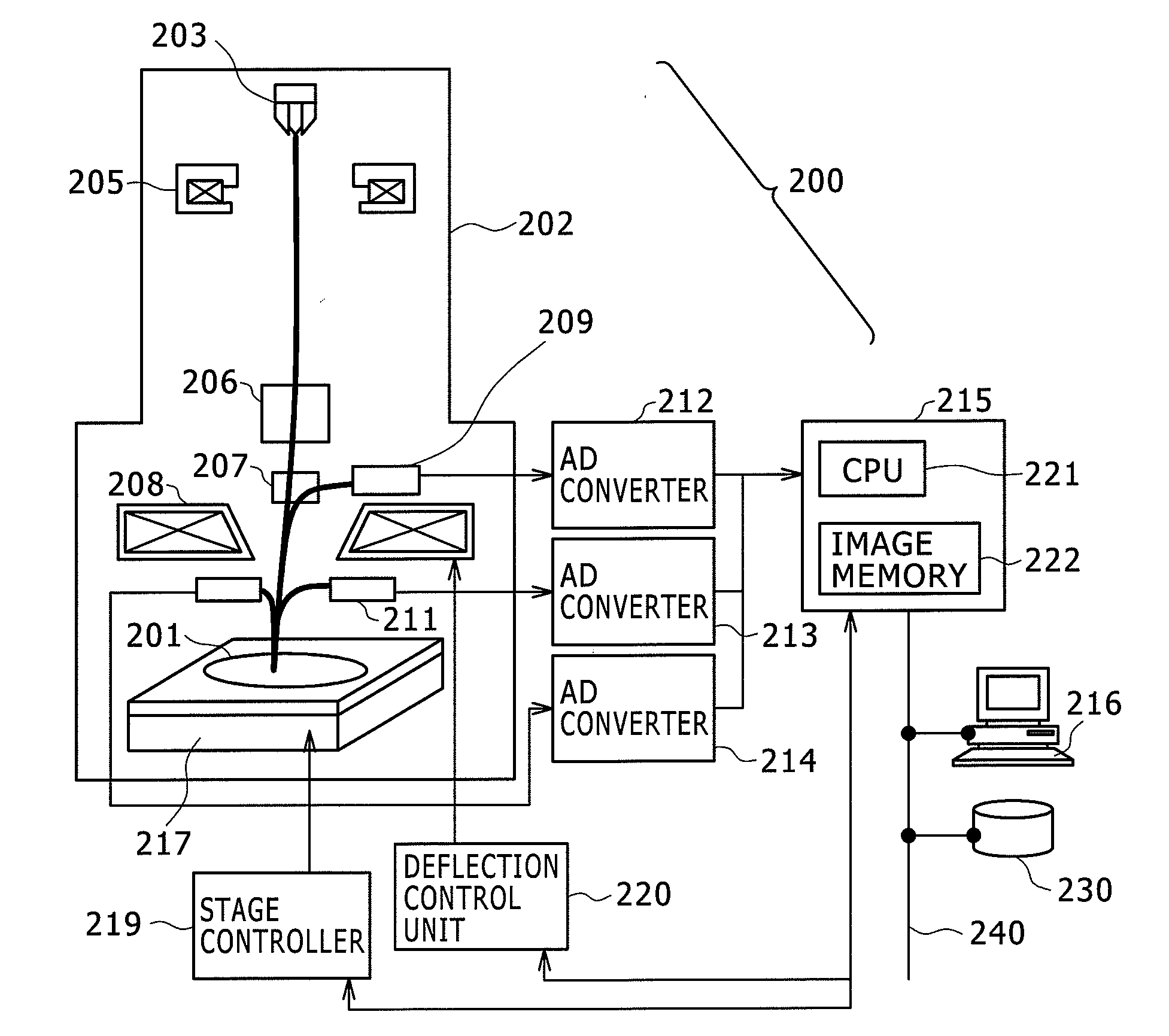
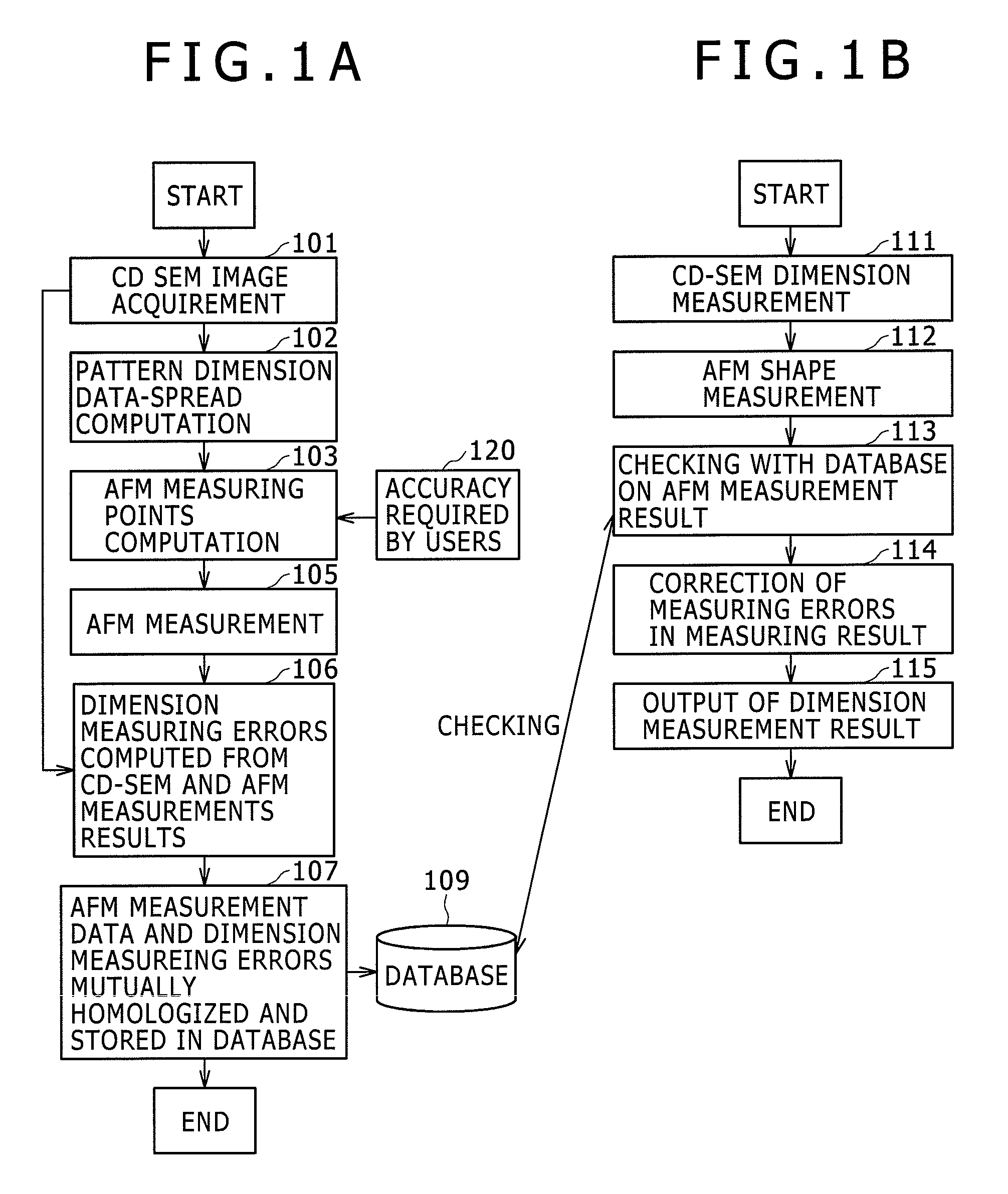
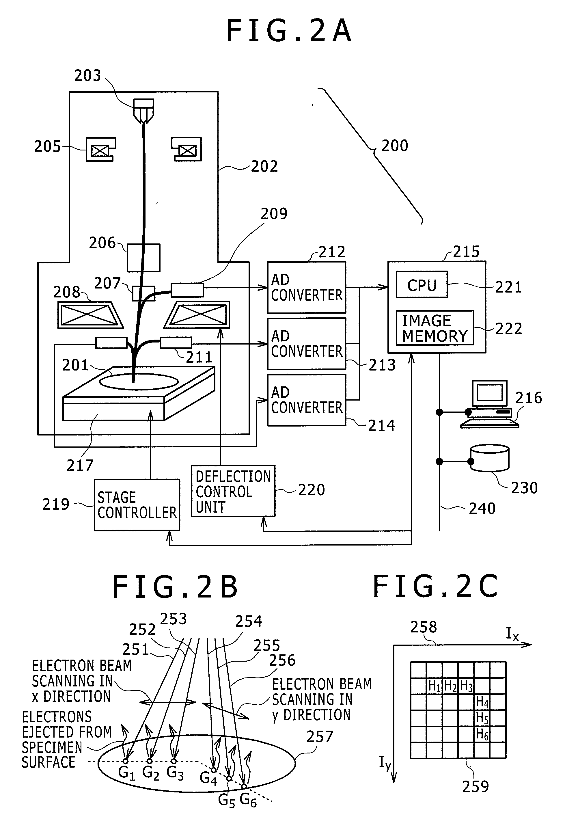
[0033][Processing Flow of Dimension Measurement of Combination of CD-SEM and AFM]

[0034]FIG. 1 shows the processing procedure of the dimension measuring means of the pattern by the CD-SEM (the block diagram is shown in FIG. 2) according to the preferred embodiment of the present invention. In the present invention, the evaluated result concerning the relations between the cross-sectional shapes obtained by the AFM measurement in patterns of various shapes and the CD-SEM signal waveforms is to be preliminarily recorded in the database. The actual measurement is conducted by using the above database, making it possible to correct any errors of the CD-SEM measurement occurring dependently on the cross-sectional ...


PUM


Abstract

In dimension measurement of semiconductor pattern by CD-SEM, the error value between dimensional measurement value and actual dimension on the pattern is much variational as it is dependent on the cross-sectional shape of the pattern, and a low level of accuracy was one time a big problem. In the present invention, a plurality of patterns, each different in shape, were prepared beforehand with AFM measurement result and patterns of the same shape measured by CD-SEM. These measurement results and dimensional errors were homologized with each other and kept in a database. For actual measurement of dimensions, most like side wall shape, and corresponding CD-SEM measurement error result are called up, and the called-up error results are used to correct CD-SME results of measurement object patterns. In this manner, it becomes possible to correct or reduce dimensional error which is dependent on cross-sectional shape of the pattern.

Description

BACKGROUND OF THE INVENTION [0001]1. Field of the Invention[0002]This invention relates to a semiconductor inspection equipment to evaluate if the circuit pattern formed on a semiconductor substrate is good for processing or not, and in particular, relates to a scanning electron microscope having the capability of measuring dimensional values of the above circuit pattern and a method of measuring pattern sizes using the same microscope.[0003]2. Description of the Related Art[0004]In the semiconductor manufacturing process, the trend concerning the circuit pattern formed on the wafer is fast moving toward microfabrication, and so much so that the process monitoring to keep watch over if the pattern formation is proceeded with exactly as designed is all the more increasing importance. According to the IRS (International Technology Roadmap for Semiconductors), the well-known roadmap for semiconductors, the wiring dimension of the finest pattern of a transistor gate is envisaged to real...

Claims


Application Information

Patent Timeline
IPC IPC(8): G01N23/00
CPCG01N23/225
Inventor NAGATOMO, WATARUSHISHIDO, CHIETANAKA, MAKI
Owner HITACHI HIGH-TECH CORP
Why Eureka
Try Eureka