Organic light emitting diode display and method of driving the same

Active Publication Date: 2009-08-27
LG DISPLAY CO LTD
View PDF5 Cites 215 Cited by
  • Summary
  • Abstract
  • Description
  • Claims
  • Application Information

AI Technical Summary

Benefits of technology

[0018]An object of the present invention is to provide an organic light emitting diode (OLED) display and a method of driving the same that increases the display quality by preventing the deterioration of a driving current caused by the deterioration of a drive thin film transistor (TFT) depending on driving time.
[0019]Another object of the present invention is to provide an OLED display and a method of driving th

Problems solved by technology

However, the emitting efficiency and luminance of the plasma display panel are low while its power consumption is high.
Hence, the display quality is deteriorated.
However, it is difficult to

Method used


Image

  • Organic light emitting diode display and method of driving the same
  • Organic light emitting diode display and method of driving the same
  • Organic light emitting diode display and method of driving the same

Examples


first exemplary embodiment

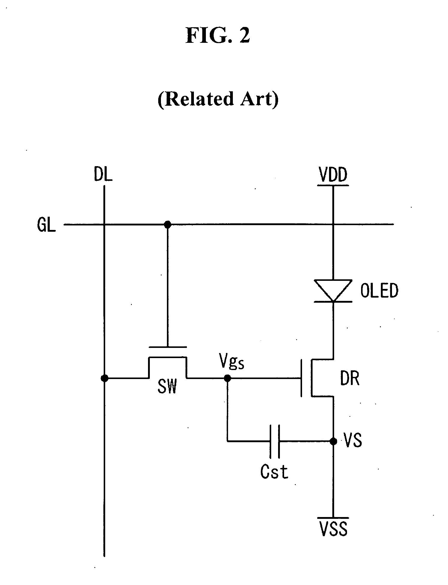
[0053]Because it is difficult to control current data depending on each gray level in an organic light emitting diode (OLED) display, a driving current actually flowing in an OLED is generated by setting a compensation voltage using a relatively high reference current and downscaling the set voltage in accordance with a first exemplary embodiment of the present invention. In the OLED display according to the first exemplary embodiment of the invention, a potential of a source electrode of a drive element is fixed at the set voltage, and a driving current is downscaled by reducing a potential of a gate electrode of the drive element from a reference voltage that is already supplied.

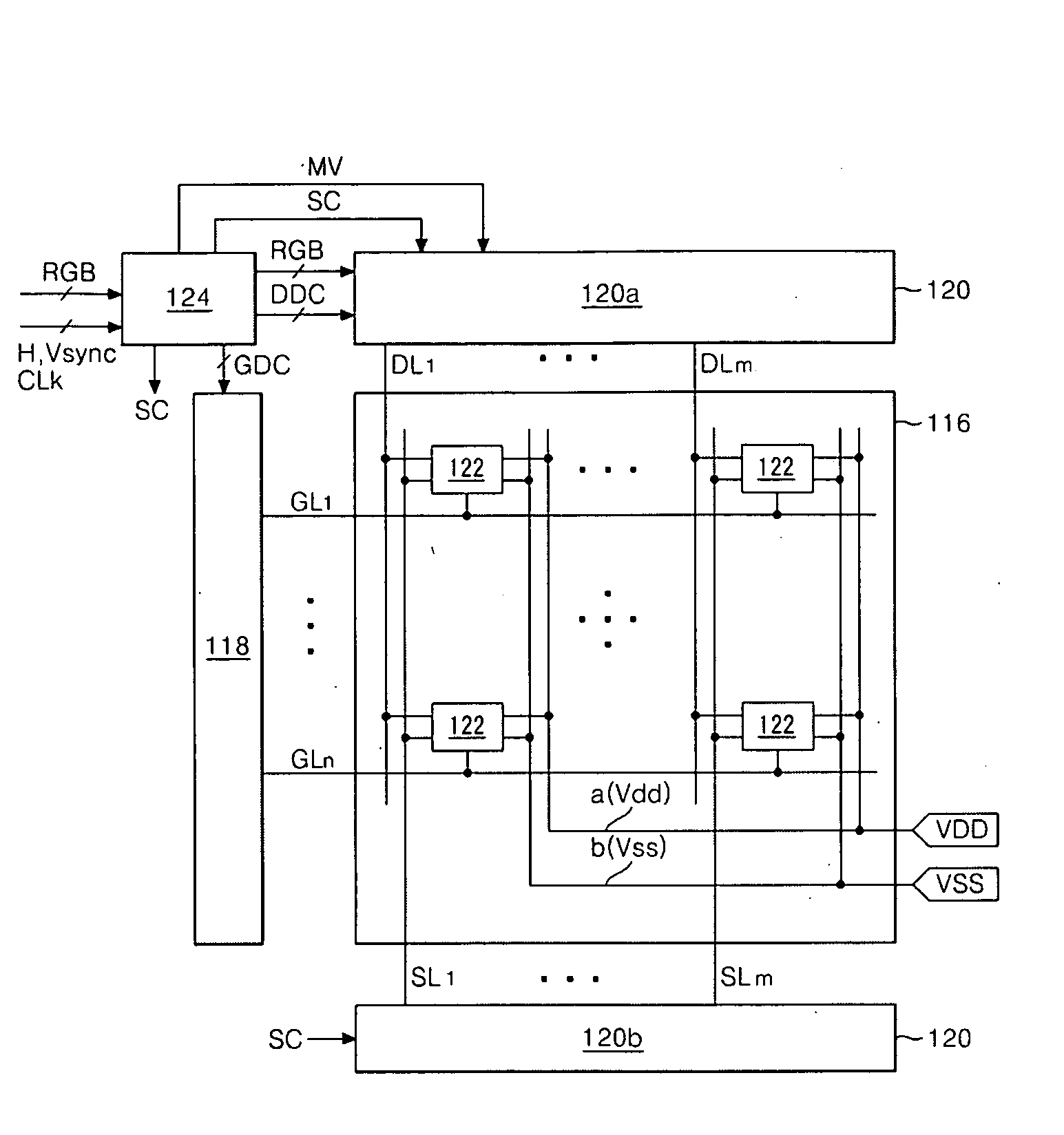
[0054]FIG. 4 is a block diagram showing an OLED display according to the first exemplary embodiment of the invention. FIG. 5 is a circuit diagram of an exemplary data drive circuit of FIG. 4.

[0055]As shown in FIGS. 4 and 5, the OLED display according to the first exemplary embodiment of the invention inclu...

second exemplary embodiment

[0082]The OLED display according to a second exemplary embodiment of the present invention fixes a potential of a gate electrode of a drive element at a reference voltage and sets a potential of a source electrode of the drive element to a compensation voltage and at the same time raises the set voltage, thereby downscaling the driving current.

[0083]FIG. 10 is a block diagram showing an OLED display according to the second exemplary embodiment of the invention. FIG. 11 is a circuit diagram of an exemplary data drive circuit of FIG. 10.

[0084]As shown in FIGS. 10 and 11, the OLED display according to the second exemplary embodiment of the invention includes a display panel 216, a gate drive circuit 218, a data drive circuit 220, and a timing controller 224. The display panel 216 includes m×n pixels 222 at each crossing region of m data lines DL1 to DLm and n gate lines GL1 to GLn. Signal lines “a” supplying a high potential driving voltage Vdd to each pixel 222, signal lines “b” suppl...

third exemplary embodiment

[0106]The OLED display according to a third exemplary embodiment of the present invention fixes a potential of a gate electrode of a drive element at a high potential driving voltage and sets a potential of a source electrode of the drive element at a compensation voltage and at the same time raises the set voltage, thereby downscaling a driving current.

[0107]FIG. 15 is a block diagram showing an OLED display according to the third exemplary embodiment of the invention. As shown in FIG. 15, the OLED display according to the third exemplary embodiment of the invention includes a display panel 316, a gate drive circuit 318, a data drive circuit 320, and a timing controller 324. The OLED display according to the third exemplary embodiment of the invention is different from the OLED display according to the second exemplary embodiment of the invention in that the connection structure of a cell drive circuit inside a pixel is different from each other, and a reference voltage source gene...


PUM


Abstract

An organic light emitting diode display includes a data line, a gate line that crosses the data line to receive a scan pulse, a high potential driving voltage source to generate a high potential driving voltage, a low potential driving voltage source to generate a low potential driving voltage, a light emitting element to emit light due to a current flowing between the high potential driving voltage source and the low potential driving voltage source, a drive element connected between the high potential driving voltage source and the light emitting element to control a current flowing in the light emitting element depending on a voltage between a gate electrode and a source electrode of the drive element, and a driving current stabilization circuit to apply a first voltage to the gate electrode of the drive element to turn on the drive element and to sink a reference current through the drive element to set a source voltage of the drive element at a sensing voltage and to modify the voltage between the gate and source electrodes of the drive element to scale a current to be applied to the light emitting element from the reference current.

Description

[0001]This application claims the benefit of Korea Patent Application No. 10-2008-0016503 filed on Feb. 22, 2008, which is incorporated herein by reference for all purposes as if fully set forth herein.BACKGROUND OF THE INVENTION[0002]1. Field of the Invention[0003]The present invention relates to an organic light emitting diode display, and more particularly to an organic light emitting diode display and a method of driving the same capable of increasing the display quality by preventing a driving current from becoming degraded by the degradation of a drive thin film transistor (TFT) depending on driving time.[0004]2. Discussion of the Related Art[0005]Recently, various kinds of flat panel display devices with reduced weight and size have been developed as a replacement of cathode ray tubes. Examples of the flat panel display devices include liquid crystal displays (LCD), field emission displays (FED), plasma display panels (PDP), and electroluminescence devices. Because the struct...

Claims


Application Information

Patent Timeline
IPC IPC(8): G09G3/30
CPCG09G3/3233G09G3/3291G09G2300/0819G09G2320/0295G09G2310/0251G09G2310/0262G09G2300/0842G09G3/30G09G3/32G09G3/20H05B33/12
Inventor NAM, WOO JIN
Owner LG DISPLAY CO LTD
Why Eureka
Try Eureka