
Metal waveguide device and NANO plasmonic integrated circuits and optical integrated circuit module using the same

a technology of integrated circuits and metal waveguides, which is applied in the direction of optical waveguide light guides, instruments, nanotechnology, etc., can solve the problems that cannot be applied to nano technology, and achieve the effects of high-integration photonics, low power consumption, and microstructur

Active Publication Date: 2009-08-27
RES & BUSINESS FOUND SUNGKYUNKWAN UNIV
View PDF2 Cites 8 Cited by
  • Summary
  • Abstract
  • Description
  • Claims
  • Application Information

AI Technical Summary

Benefits of technology

[0010]Therefore, the present invention has been made keeping in mind the problems encountered in the related art and provides a metal waveguide device, and nano plasmonic integrated circuits and an optical integrated circuit module using the same, thus realizing highly integrated photonic circuits having a micro structure, low power consumption, low price and a disposable use.

Problems solved by technology

However, the OADM module and the photonic crystal integrated circuit module do not correspond to sub-micro devices which are under active study these days, and thus cannot be applied to nano technology.

Method used


Image

  • Metal waveguide device and NANO plasmonic integrated circuits and optical integrated circuit module using the same
  • Metal waveguide device and NANO plasmonic integrated circuits and optical integrated circuit module using the same
  • Metal waveguide device and NANO plasmonic integrated circuits and optical integrated circuit module using the same

Examples


Embodiment Construction

[0042]Hereinafter, a detailed description will be given of nano plasmonic integrated circuits and an optical integrated circuit module using the same according to the present invention.

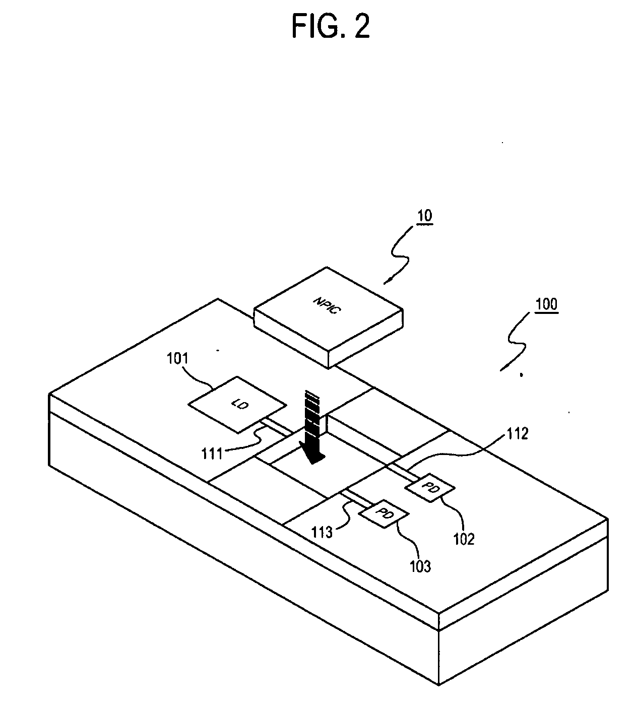
[0043]The concept of nano plasmonic integrated circuits will now be described first. The nano plasmonic integrated circuit is a circuit formed by integrating a series of devices into one sub-mm sized chip, the series of devices being responsible for converting incident optical signals into SPP signals or producing them, transmitting the SPP signals through a waveguide, recognizing or sensing and processing the transmitted SPP signals, and converting the SPP signals back into the optical signals, which are then output. Below, the construction of the nano plasmonic integrated circuit is specifically described with reference to the drawing.

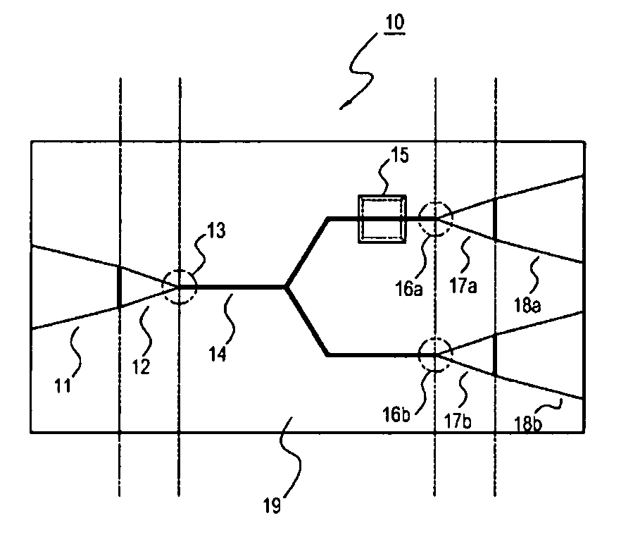
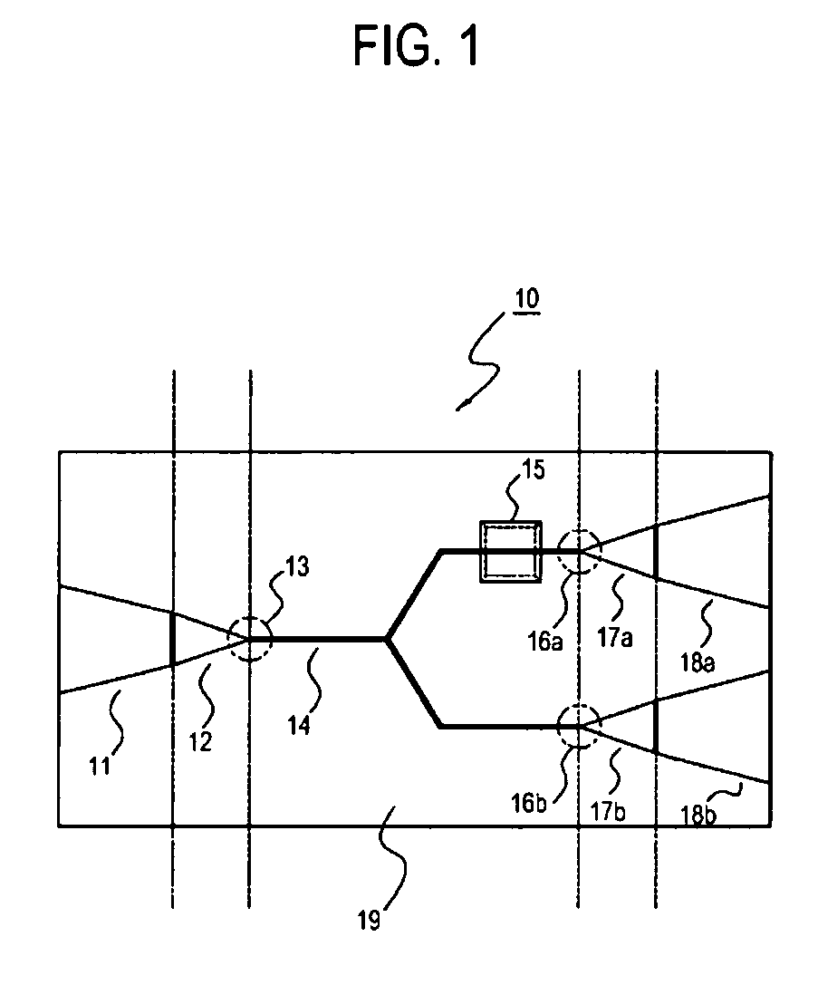
[0044]FIG. 1 shows the construction of a nano plasmonic integrated circuit module according to an embodiment of the present invention.

[0045]As shown in FIG. 1, the nan...


PUM


Abstract

Disclosed is a metal waveguide device, and nano plasmonic integrated circuits and an optical integrated circuit module using the same. The nano plasmonic integrated circuit module includes an input coupling unit, an input focusing unit, a surface plasmon polariton waveguide for guiding surface plasmon polaritons, a signal sensing / processing unit, an output defocusing unit, and an output coupling unit for converting surface plasmon polariton signals into optical signals. The optical integrated circuit module includes the nano plasmonic integrated circuit module, thus realizing highly integrated photonic circuits having a micro structure, low power consumption and low price.

Description

CROSS-REFERENCE TO RELATED APPLICATION[0001]This application claims priority to and the benefit of Korean Patent Application Nos. 10-2008-0017307 filed in the Korean Intellectual Property Office on Feb. 26, 2008 and 10-2009-0003057 filed in the Korean Intellectual Property Office on Jan. 14, 2009, the entire contents of which are incorporated herein by reference.BACKGROUND OF THE INVENTION[0002]1. Field of the Invention[0003]The present invention relates to a metal waveguide device, and nano plasmonic integrated circuits and an optical integrated circuit module using the same. More particularly, the present invention relates to a nano plasmonic integrated circuit module for converting optical signals into surface plasmon polariton (SPP) signals, transmitting the converted SPP signals, and sensing and processing the transmitted SPP signals.[0004]2. Description of the Related Art[0005]Recently, it has been experimentally confirmed that when a metal and a dielectric satisfy specific co...

Claims


Application Information

Patent Timeline
IPC IPC(8): G02B6/10G02B6/12
CPCG02B6/1226B82Y20/00
Inventor HYUN, LEE MYUNGRYEONG, PARK HAE
Owner RES & BUSINESS FOUND SUNGKYUNKWAN UNIV
Learn More