Semiconductor device and method of fabricating the same

Inactive Publication Date: 2009-09-03
PANASONIC CORP
View PDF13 Cites 32 Cited by
  • Summary
  • Abstract
  • Description
  • Claims
  • Application Information

AI Technical Summary

Benefits of technology

[0021]Therefore, an object of the present invention is to provide a semiconductor device capable of preventing a crack caused by stress concentrated on one position from being generated by reducing the deformation of semiconductor chips due to the shrinkage of sealing resin, even if each semiconductor chip to be stacked on the semiconductor device is designed to be thinner, capable of reali

Problems solved by technology

Furthermore, for realizing the further reduced thickness, size and weight of a semiconductor package, a wafer level chip size package (WLCSP) has been proposed instead of a bare chip and has become widely used recently, since the bare chip is not easy to use when mounting the chip to an electrical apparatus.
However, due to a difference between a thermal expansion coefficient of each semiconductor chip and a thermal expansion coefficient of sealing resin injected between semiconductor chips, a distortion or a crack generated in the semiconductor chip has been an issue.
Note that this problem is not so much concerned in the flip-chip mounting of a single semiconductor chip since the thickness thereof is sufficient enough to have stiffness.
However, this problem is of great concern in the flip-chip mounting of a semiconductor chip having a three-dimensional stacked structure.
However, in the case where three or more semiconductor chips are stacked in layers, the closer to the top a semiconductor chip is disposed, t

Method used


Image

  • Semiconductor device and method of fabricating the same
  • Semiconductor device and method of fabricating the same
  • Semiconductor device and method of fabricating the same

Examples


first embodiment

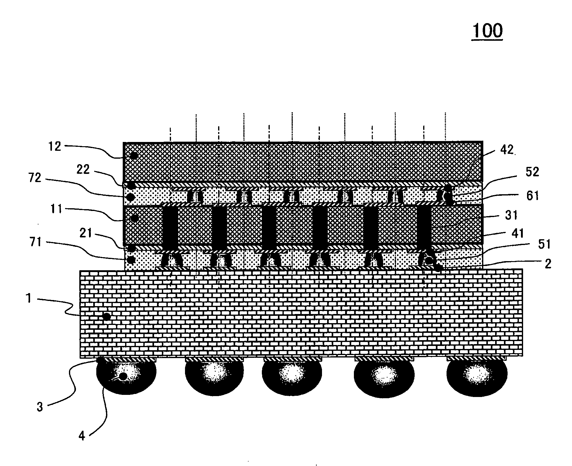
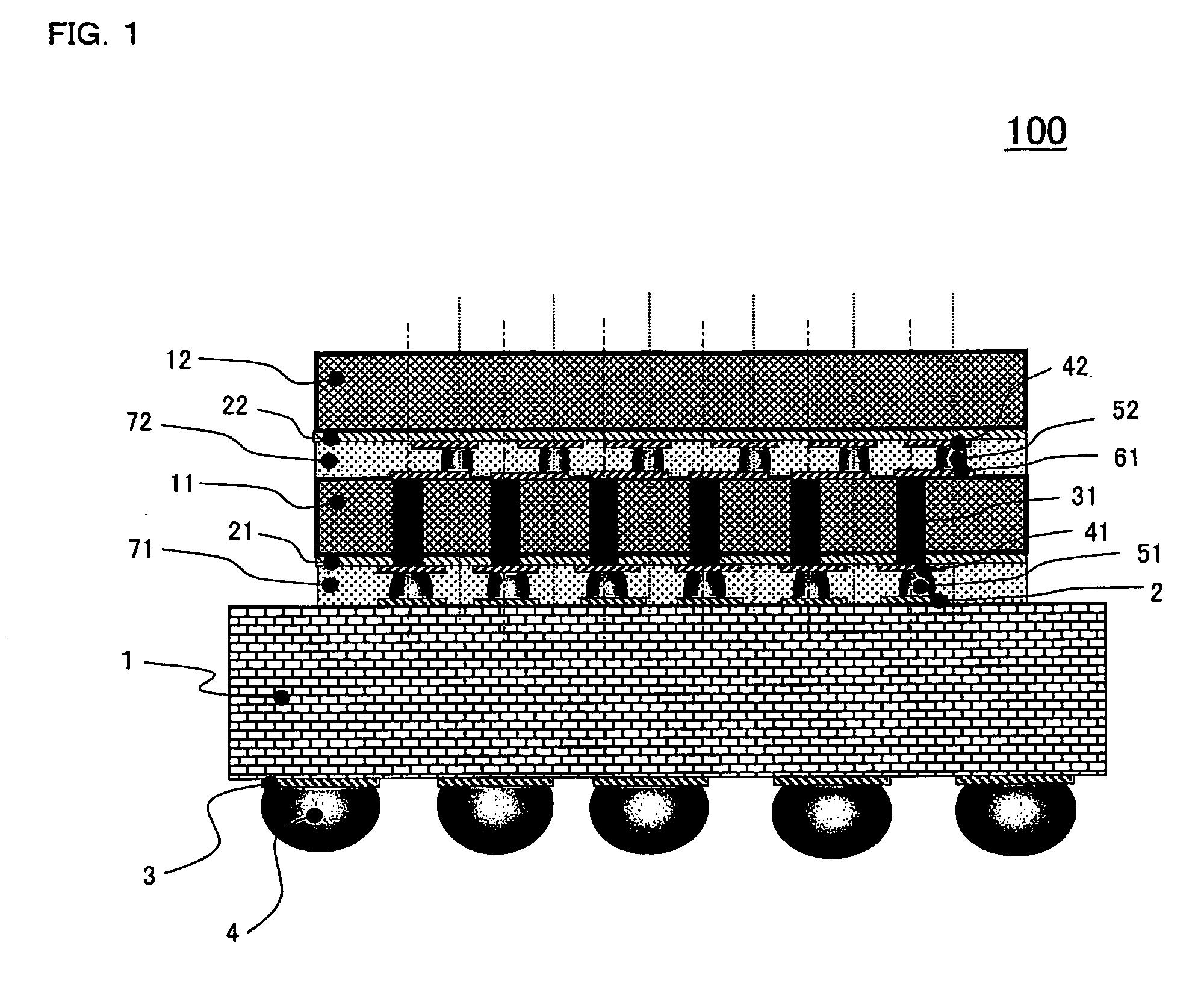
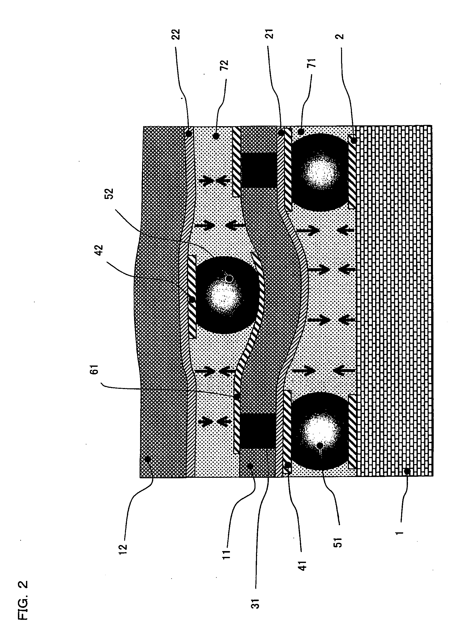
[0100]A structure of a semiconductor device according to a first embodiment of the present invention is basically the same as that of the semiconductor device 1000 according to the prior art shown in FIGS. 28 and 29. The semiconductor device according to the first embodiment of the present invention is the same as the semiconductor device 1000 according to the prior art except for arrangement positions of a through via, an electrode pad and a bump. In the semiconductor device 1000 according to the prior art, a position at which a through via, an electrode pad and a bump are arranged on one semiconductor chip is the same as a position at which the above three components are arranged on another semiconductor chip. In contrast, in the semiconductor device according to the first embodiment of the present invention, a position at which a through via, an electrode pad and a bump are arranged on one semiconductor chip is shifted from a position at which the above three components are arran...

second embodiment

[0117]A structure of the semiconductor device according to a second embodiment of the present invention is basically the same as that according to the first embodiment of the present invention. Specifically, positions at which through vias are formed on each semiconductor chip are different between the first and second embodiments. In the semiconductor device according to the first embodiment of the present invention, on the circuit element surface of each of the semiconductor chips stacked in multi-layers, the electrode pad is arranged at a position at which the through via is formed so as to form the bump on the circuit element surface. In contrast, in the semiconductor device according to the second embodiment of the present invention, the bump is formed at a position shifted from a position at which the through via is formed on each of the semiconductor chips stacked in multi-layers. Hereinafter, the detailed structure of the semiconductor device according to the second embodime...

third embodiment

[0124]A structure of the semiconductor device according to a third embodiment of the present invention differs from that of the semiconductor device according to the first embodiment of the present invention in that in the semiconductor according to the third embodiment, a resin layer is additionally provided around the periphery of each bump.


PUM


Abstract

In a semiconductor device of the present invention, semiconductor chips are stacked in multi-layers. Each of the semiconductor chip includes: through vias extending through a top main surface thereof to a bottom surface opposite to the top main surface; a circuit element surface formed on the top main surface; pads arranged on the circuit element surface; bumps formed on the pads; and via pads, formed on the bottom surface thereof, to which the bumps of its upper semiconductor chip are joined, and positions at which the bumps of each of the semiconductor chips are respectively arranged are different from those at which the bumps of its upper semiconductor chip are arranged.

Description

BACKGROUND OF THE INVENTION[0001]1. Field of the Invention[0002]The present invention relates to a semiconductor device, and more particularly to a semiconductor device having a package structure in which a plurality of semiconductor chips are three-dimensionally stacked and a method of fabricating the same.[0003]2. Description of the Background Art[0004]In recent years, for further reducing the thickness, size and weight of electrical apparatuses (cellular phones and the like), a package of the semiconductor device has been shifted from a peripheral lead type package to a Ball Grid Array (BGA) type package and further to a chip size package (CSP). The CSP technology provides a semiconductor package (semiconductor device) having an area substantially equivalent to that of each individual chip cutout from a wafer. Furthermore, for realizing the further reduced thickness, size and weight of a semiconductor package, a wafer level chip size package (WLCSP) has been proposed instead of a...

Claims


Application Information

Patent Timeline
IPC IPC(8): H01L25/00H01L21/48
CPCH01L21/563H01L2224/16235H01L24/16H01L24/17H01L24/48H01L24/73H01L25/0657H01L2224/13099H01L2224/16H01L2224/2518H01L2224/48227H01L2224/48235H01L2224/73203H01L2225/0651H01L2225/06513H01L2225/06527H01L2225/06541H01L2225/06562H01L2225/06582H01L2924/01029H01L2924/01078H01L2924/01079H01L2924/01082H01L2924/15311H01L2924/01006H01L2924/01033H01L2924/01047H01L2924/014H01L2924/10253H01L23/49816H01L2924/00H01L2224/02372H01L2224/73204H01L2224/73257H01L2924/00014H01L2924/181
Inventor KUWABARA, KIMIHITO
Owner PANASONIC CORP
Why Eureka
Try Eureka