Resonant Element and Method for Manufacturing the Same

a technology of resonant elements and manufacturing methods, applied in the field of resonant elements, can solve the problems of increasing manufacturing costs and uneven amount of solder on the respective side surfaces, and achieve the effects of reducing the influence on the length of the resonator, easy adjustment, and easy adjustmen

Inactive Publication Date: 2009-09-03
MURATA MFG CO LTD
View PDF4 Cites 0 Cited by
  • Summary
  • Abstract
  • Description
  • Claims
  • Application Information

AI Technical Summary

Benefits of technology

[0015]The first and second side-surface electrode patterns may be provided with a plurality of side-surface electrodes that are in conduction with the same principal-surface electrode. In this configuration, it is easy to place the respective side-surface electrode patterns in a point-symmetric manner and to form the side-surface electrode patterns that match each other on the side surfaces facing each other. Also, if there are other adjacent side-surface electrodes on the outer side of the above-described plurality of side-surface electrodes, electromagnetic-field coupling occurs between the plurality of side-surface electrodes and the other side-surface electrodes. Thus, in this configuration, the frequency characteristic can be easily adjusted by causing a significant change in electromagnetic-field coupling, particularly multipath coupling, through adjustment of gaps between those side-surface electrodes.
[0016]The principal-surface electrode that is in conduction with the plurality of side-surface electrodes may have a wide end portion that is in conduction with the plurality of side-surface electrodes. With this configuration, even if a cut error occurs at cutting of a mother substrate into dielectric substrates, no influence is exerted on a narrow portion of the principal-surface electrode and thus an influence on the resonator length reduces.
[0017]Dummy electrodes separated from the principal-surface electrode constituting part of the resonators may be provided in the first and second side-surface electrode patterns. In this configuration, the dummy electrodes easily enable formation of point-symmetric side-surface electrode patterns and side-surface electrode patterns that match each other on the side surfaces facing each other. If the position where the dummy electrodes are formed is close to the principal-surface electrode constituting the resonators, end capacitance is added to the principal-surface electrode. Thus, in this configuration, the frequency characteristic can be easily adjusted by causing a significant change in end capacitance through adjustment of gaps between the dummy electrodes and the principal-surface electrode.
[0018]As the principal-surface electrode pattern, an end capacitance electrode that continues to the dummy electrodes and that causes end capacitance to be generated in the principal-surface electrode constituting the resonators may be provided. In this configuration, the gap between the end capacitance electrode and the principal-surface electrode is constant even if a cut error occurs at cutting of a mother substrate into dielectric substrates. Therefore, variations in end capacitance can be reduced and an influence of the cut error exerted on the resonance characteristic can be reduced.
[0019]A side-surface electrode pattern that is point-symmetric in the side surface is formed on side surfaces placed on a printing surface of a pallet of dielectric substrates placed in holding holes of the pallet, and a side-surface electrode pattern having the same form is formed on the facing side surface, whereby resonant elements are manufactured. Accordingly, side-surface electrode patterns can be formed on the two side surfaces facing each other by using the same printing pattern, so that the process of aligning the resonant elements can be simplified.
[0020]According to the present invention, a process of aligning a plurality of resonant elements before forming of side surface electrodes is simplified. Accordingly, the manufacturing cost can be suppressed. Also, the risk of displacement of positions where resonant elements are mounted during a mounting process can be reduced, so that connection failure or characteristic failure can be suppressed.

Problems solved by technology

This process is sophisticated, e.g., the process is performed with the use of an aligning apparatus to recognize and correct respective orientations of a plurality of elements by using an image recognizing technique, thereby increasing the manufacturing cost.
Furthermore, when such a resonant element is mounted on a substrate, the amounts of solder on the respective side surfaces are uneven due to asymmetry of the positions of the side-surface electrodes.

Method used


Image

  • Resonant Element and Method for Manufacturing the Same
  • Resonant Element and Method for Manufacturing the Same
  • Resonant Element and Method for Manufacturing the Same

Examples


Embodiment Construction

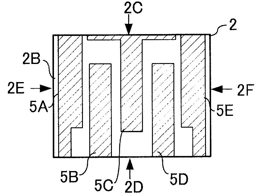
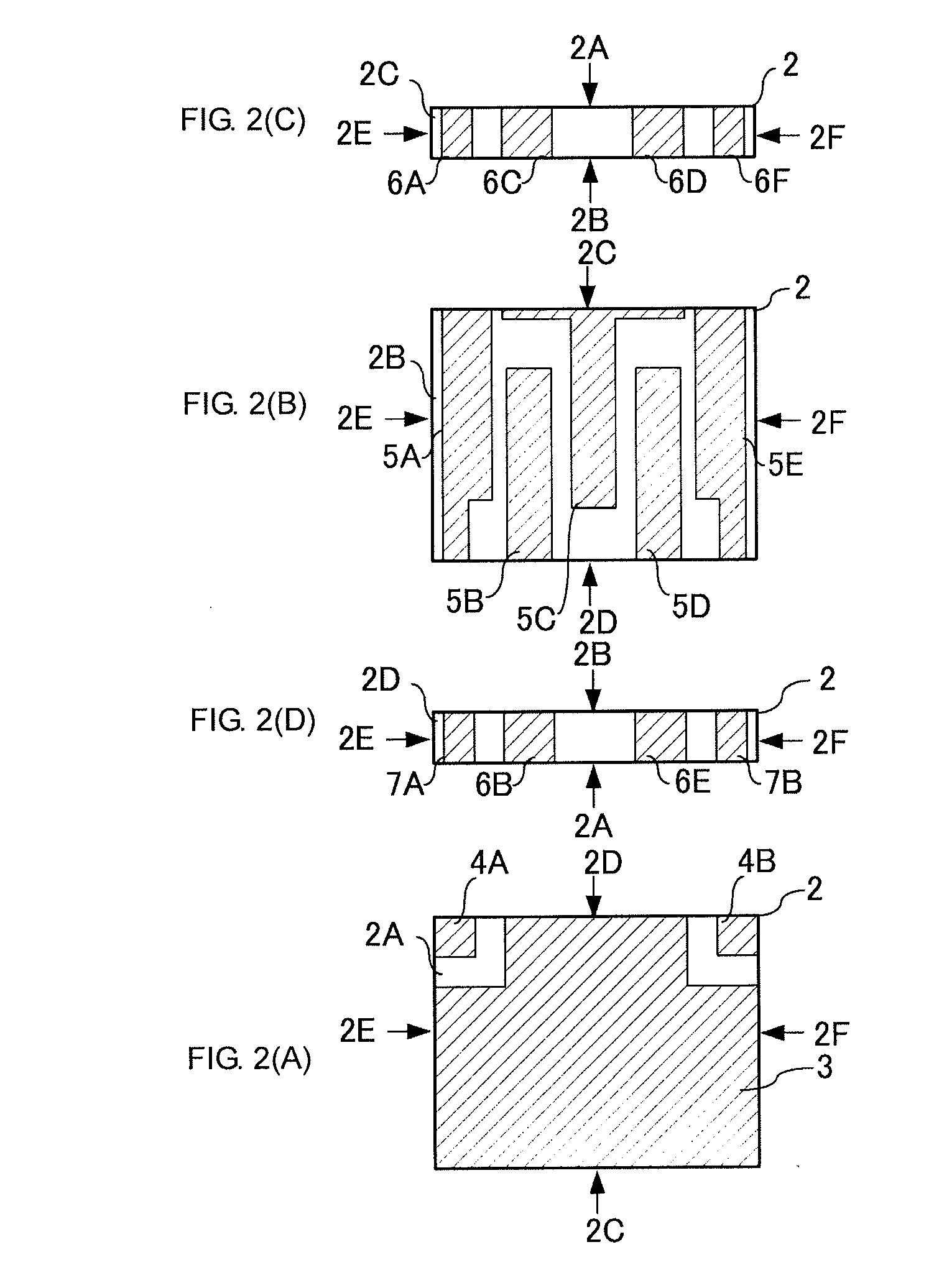
[0046]Hereinafter, the present invention is described on the basis of configuration examples of a resonant element. FIGS. 2(A)-2(D) are partial developed views of a resonant element. This resonant element includes stripline resonators and is used as a filter that is used for UWB (Ultra Wide Band) communication of high frequencies in a wide band.

[0047]This resonant element includes a dielectric substrate 2 having a compact rectangular parallelepiped shape. The dielectric substrate 2 is made of a ceramic dielectric material, such as titanium oxide. The dielectric substrate 2 has a relative permittivity of about 110, a thickness of 500 μm, a dimension in a lateral direction in the figures of about 3.2 mm, and a dimension in a short-side direction of principal surfaces of about 2.5 mm.

[0048]The composition and dimensions of the dielectric substrate 2 may be appropriately set in view of a frequency characteristic and so on.

[0049]A rear principal surface 2A of the dielectric substrate 2 i...


PUM

PropertyMeasurementUnit
thicknessaaaaaaaaaa
thicknessaaaaaaaaaa
thicknessaaaaaaaaaa

Abstract

A plurality of flat-plate filter elements are placed on a pallet having a plurality of holding holes. Each of the filter elements includes a rear-principal-surface electrode pattern having a ground electrode provided on a rear principal surface and a front-principal-surface electrode pattern having a principal-surface electrode provided on a front principal surface. One of a first side surface and a second side surface of each of the filter elements is placed on a printing surface of the pallet. A first side-surface electrode pattern of a point-symmetric form in the side surfaces is formed on the side surfaces placed on the printing surface of the pallet. Then, the filter elements are vertically inverted, and a second side-surface electrode pattern having the same form as the first side-surface electrode pattern is formed on the side surfaces facing each other.

Description

CROSS REFERENCE TO RELATED APPLICATIONS[0001]The present application is a continuation of International Application No. PCT / JP2007 / 071964, filed Nov. 13, 2007, which claims priority to Japanese Patent Application No. JP2007-023461, filed Feb. 1, 2007, the entire contents of each of these applications being incorporated herein by reference in their entirety.FIELD OF THE INVENTION[0002]The present invention relates to a resonant element including quarter-wavelength stripline resonators provided on a dielectric substrate, and to a method for manufacturing the resonant element.BACKGROUND OF THE INVENTION[0003]A resonant element, such as a filter or a balun, including stripline resonators provided on a dielectric substrate has been used (e.g., see Patent Document 1).[0004]Now, a configuration of a conventional resonant element is described by using a filter as an example. FIG. 1 is a developed view of a conventional filter.[0005]A resonant element 101 is constituted through interdigital ...

Claims


Application Information

Patent Timeline
Patent Type & Authority Applications(United States)
IPC IPC(8): H01P3/08H05K3/10
CPCH01P1/20336Y10T29/49155H01P11/007
Inventor TUJIGUCHI, TATSUYATAKEI, YASUNORIHONDA, NOBUYOSHI
Owner MURATA MFG CO LTD
Why Eureka
Try Eureka