Semiconductor device, semiconductor device manufacturing method and lid frame

a semiconductor device and manufacturing method technology, applied in the direction of fluid pressure measurement, fluid pressure measurement by electric/magnetic elements, instruments, etc., can solve the problems of reducing the reliability increasing the cost of manufacturing a semiconductor device, and reducing the manufacturing efficiency of the semiconductor device, so as to improve the manufacturing efficiency and reduce costs.

Inactive Publication Date: 2009-09-17
YAMAHA CORP
View PDF5 Cites 142 Cited by
  • Summary
  • Abstract
  • Description
  • Claims
  • Application Information

AI Technical Summary

Benefits of technology

[0039]As a result, according to the present invention, it is no longer necessary to perform a step to fix the lid frame which covers the semiconductor chip to the circuit board, or to perform a step of forming through holes in the circuit board. As a resu

Problems solved by technology

Because of this, the problem arises that manufacturing the circuit board becomes somewhat complex, which leads to a reduction in the manufacturing efficiency of a semiconductor device.
In addition, there is an increase in the cost of manufacturing a semiconductor device.
When this cover is placed in position, the problem has arisen that it sometimes comes into contact with the semiconductor sensor chip and amplifier or with the wires electrically connecting them and thus causing damage.
Moreover, because distal end portions of the cover are fixed to the printed circuit using only, for example, an adhesive agent, if, for example, a shock or the like is applied thereto, the cover sometimes comes off, so that the problem and has arisen that

Method used


Image

  • Semiconductor device, semiconductor device manufacturing method and lid frame
  • Semiconductor device, semiconductor device manufacturing method and lid frame
  • Semiconductor device, semiconductor device manufacturing method and lid frame

Examples


first embodiment

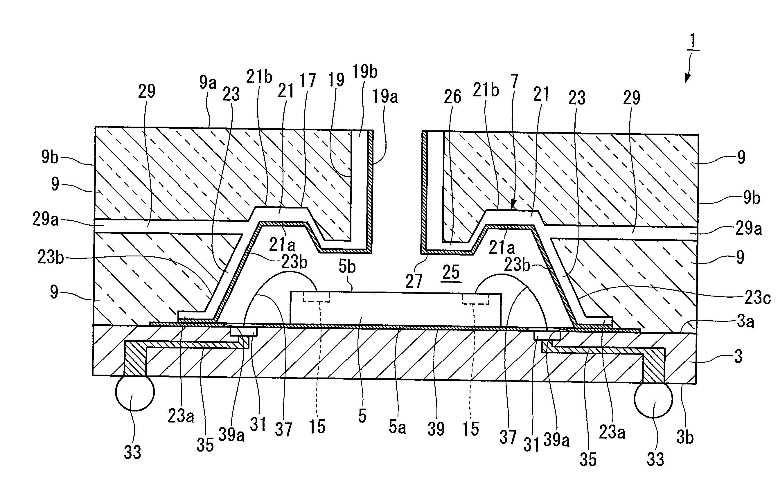
[0081]the present invention is shown in FIG. 1 through FIG. 5. As is shown in FIG. 1, this semiconductor device 1 is provided with a circuit board 3, a semiconductor chip 5 that is superimposed on one end side in the thickness direction of the circuit board 3, a lid frame 7, and a resin mold portion 9.

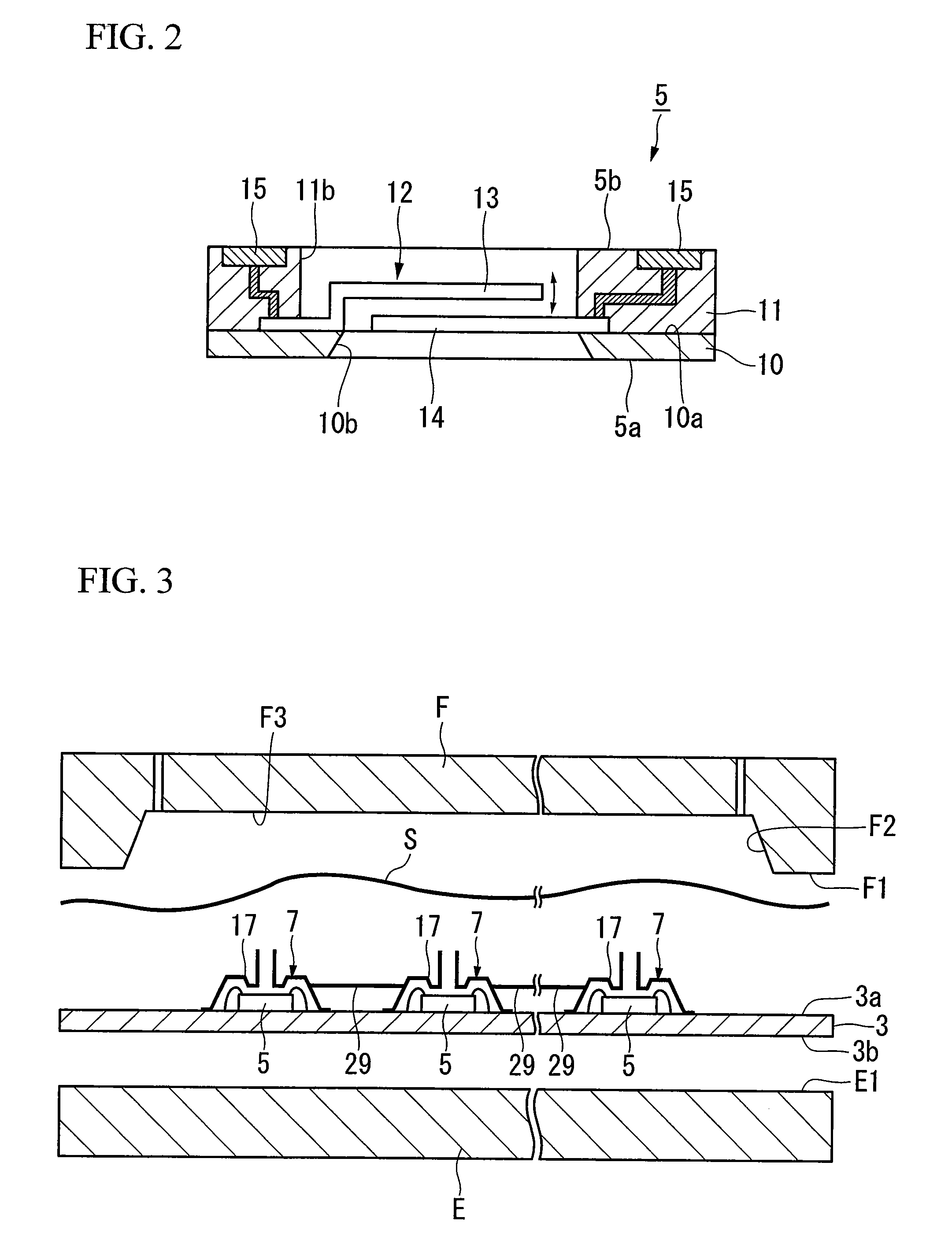
[0082]The semiconductor chip 5 is formed substantially in a plate shape, and a rear surface 5a thereof is adhesively fixed to a front surface 3a that is positioned on the one end side of the circuit board 3. This semiconductor chip 5 is, for example, a sound pressure sensor chip.

[0083]Namely, as is shown in FIG. 2, this semiconductor chip 5 is constructed by stacking a multilayer printed circuit board 11 on a surface 10a of a silicon substrate 10, and then providing a condenser unit 12 in through holes 10b and 11b that penetrate in the thickness direction the silicon substrate 10 and the multilayer printed circuit board 11. The condenser unit 12 is formed by an oscillating electrode pl...

third embodiment

[0153]FIG. 8 through FIG. 13 show the present invention. As is shown in FIG. 8 through FIG. 10, a semiconductor device 101 is provided with a metal stage portion 103 that is formed substantially in a plate shape, a plurality of metal electrical connection leads 105 and a connecting lead 106 that are placed around the stage portion 103, a semiconductor chip 107, an IC 109, and a through electrode 111 that are placed on a rear surface (i.e., one surface) 103a of the stage portion, a chip covering lid body 113 that is placed on the rear surface 103a of the stage portion 103, a stage covering lid body 115 that is placed on a front surface (i.e., another surface) 103b of the stage portion 103, and a resin mold portion 117 that fixes the stage portion 103, the leads 105 and 106, the chip covering lid body 113, and the stage covering lid body 115 in a single integral unit.

[0154]The stage portion 103 is formed substantially in a rectangular shape when seen in plan view, and a plurality of c...

fourth embodiment

[0215]In the structure of the fourth embodiment shown in FIG. 18 through FIG. 20, the covering portion 191 is formed on the stage covering lid body 189, however, the present invention is not limited to this and it is sufficient if the semiconductor device 197 is structured such that at least the molten resin does not enter into the first space portion 183. Namely, it is also possible, for example, for a non-conductive screening seal that covers the gap between the respective leads 181 and the stage portion 187 to be adhered onto a front surface (i.e., the other surface) 187b of the stage portion 187 and the leads 181. In the case of this structure, by applying the structure of the semiconductor device shown in FIG. 16, both the stage covering lid body 189 and the stage lid body placement step are rendered unnecessary.

[0216]Moreover, in the above described embodiment, the first space portion 133 that encloses the semiconductor chip 107 is sealed off from the outside, however, as is s...


PUM


Abstract

A semiconductor device includes: a substrate; a semiconductor chip that is fixed to a first surface of the substrate; a chip covering lid body that is provided on the first surface of the substrate so as to cover the semiconductor chip and that forms a hollow first space portion that surrounds the semiconductor chip, and in which there is provided a substantially cylindrical aperture portion that extends to the outer side of the first space portion and has an aperture end at a distal end thereof and that is connected to the first space portion; and a first resin mold portion that forms the first space portion via the chip covering lid body and covers the substrate such that the aperture end is exposed, and that fixes the substrate integrally with the chip covering lid body.

Description

TECHNICAL FIELD[0001]This invention relates to a semiconductor device that is provided with a semiconductor chip such as a sound pressure sensor chip and a pressure sensor chip, and to a method of manufacturing the same, and to a lid frame that is used with the same.[0002]Priority is claimed on Japanese Patent Application Nos. 2005-74901, filed Mar. 16, 2005, 2005-138371, filed May 11, 2005, 2005-197440, filed Jul. 6, 2005, and 2005-247498, filed Aug. 29, 2005, the contents of which are incorporated herein by reference.BACKGROUND ART[0003]Conventionally, semiconductor devices such as, for example, pressure sensors and silicon microphones that are manufactured using silicon semiconductors are formed substantially in a rectangular plate shape, and are provided with semiconductor sensor chips in which recessed portions are formed that are recessed from the front surface towards the rear surface thereof. In this type of semiconductor device, this semiconductor sensor chip is packaged on...

Claims


Application Information

Patent Timeline
IPC IPC(8): H01L29/84H01L23/58H01L23/538H01L23/04H01L21/50
CPCB81B7/0061B81B2201/0264H01L2924/07802B81B7/0064H01L2224/73265H01L2924/12041H01L2924/01066H01L2924/01023H01L2924/01006B81C1/00333H01L21/561H01L21/568H01L24/97H01L2221/68331H01L2224/48091H01L2224/48137H01L2224/49171H01L2224/97H01L2924/01004H01L2924/01029H01L2924/01033H01L2924/01046H01L2924/01047H01L2924/01074H01L2924/01078H01L2924/01079H01L2924/01082H01L2924/14H01L2924/15311H01L2924/19041H01L2924/30105H01L2924/3025H01L2924/01005H01L2224/85H01L2924/00014H01L2924/00H01L2924/15174H01L23/02H04R19/04
Inventor SAITOH, HIROSHISUZUKI, TOSHIHISAOMURA, MASAYOSHI
Owner YAMAHA CORP
Why Eureka
Try Eureka