Exposure method, exposure apparatus, and method of manufacturing device

a manufacturing method and exposure technology, applied in the field of exposure methods, can solve the problems of reducing affecting the performance of semiconductor devices, and affecting the yield of semiconductor devices, and achieving the effect of high overlay accuracy, high throughput, and cost reduction

Inactive Publication Date: 2009-09-17
CANON KK
View PDF2 Cites 11 Cited by
  • Summary
  • Abstract
  • Description
  • Claims
  • Application Information

AI Technical Summary

Benefits of technology

[0014]It is, therefore, an object of the present invention to correct the overlay error amount of a substrate with high overlay accuracy and high throughput without any increase in cost.

Problems solved by technology

This is a factor that degrades the performance of a semiconductor device and the yield of semiconductor device manufacture.
Another error factor in wafer alignment is a TIS (Tool Induced Shift) in an alignment detection system.
A WIS and a TIS and the synergistic effect between them degrade the overlay accuracy of wafers.
With regard to the same real device wafer, therefore, the exposure offset obtained by a given exposure apparatus cannot be applied as an exposure offset to another exposure apparatus.
In consideration of the total throughput in the manufacture of semiconductor devices, however, it is not desirable that all the exposure apparatuses which will be used to expose the same real device wafer respectively obtain exposure offsets, in spite of the fact that the same real device wafer is exposed.
In addition, in order to allow all the exposure apparatuses to respectively obtain exposure offsets, a plurality of overlay inspection apparatuses are required, resulting in an increase in cost.
In this case, since the TISs in the alignment detection systems in the respective exposure apparatuses differ from each other, the alignment accuracy deteriorates.
For this reason, the performance of semiconductor devices and the yield of semiconductor device manufacture decrease.

Method used


Image

  • Exposure method, exposure apparatus, and method of manufacturing device
  • Exposure method, exposure apparatus, and method of manufacturing device
  • Exposure method, exposure apparatus, and method of manufacturing device

Examples


Embodiment Construction

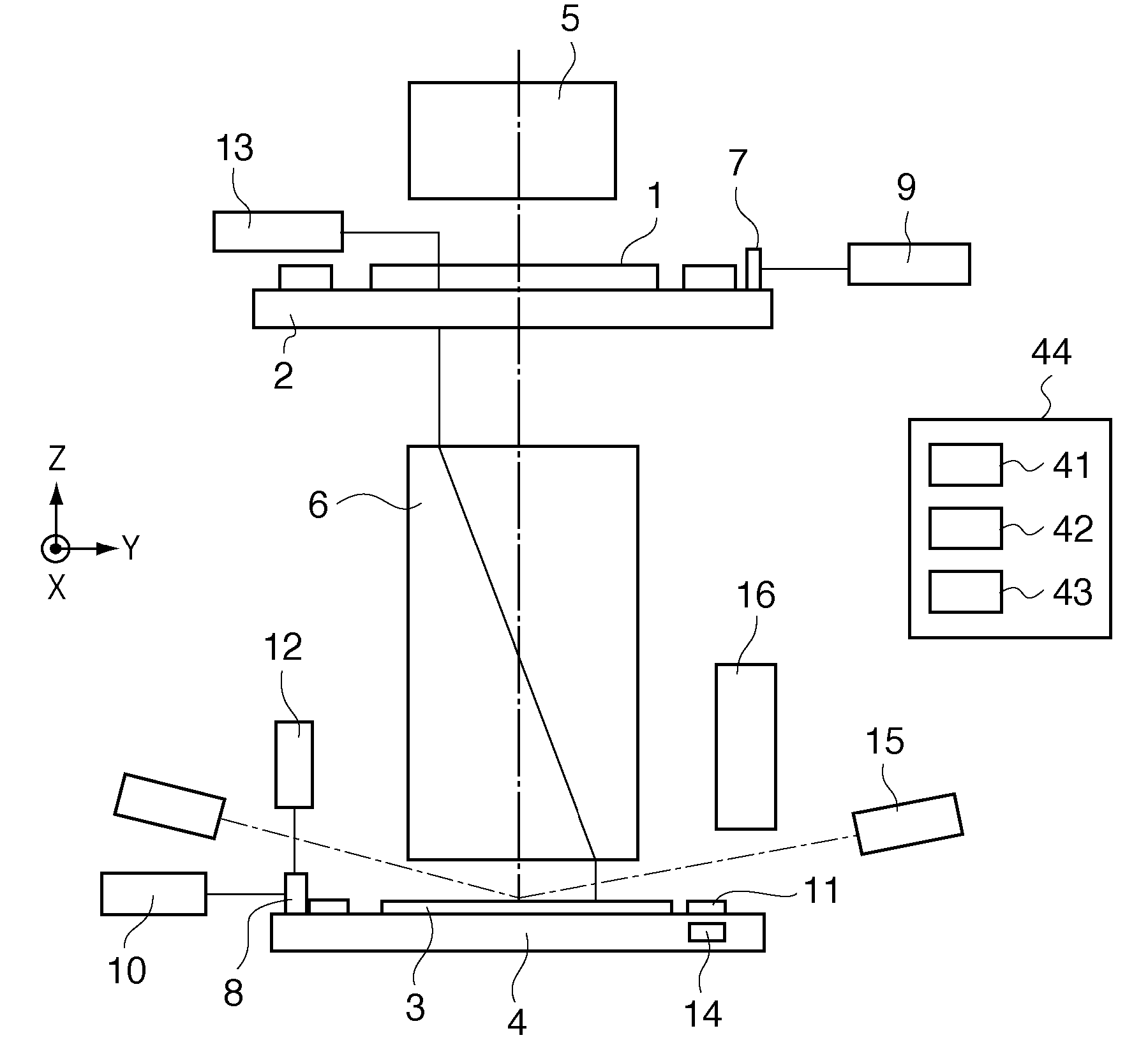
[0032]It is an object of the present invention to provide an exposure apparatus which can correct the overlay error amount of a substrate (wafer) with high overlay accuracy and high throughput. This invention is characterized in that once a given exposure apparatus obtains an exposure offset for a given real device wafer, all the exposure apparatuses which are going to perform alignment by using the real device wafer calculate exposure offsets without causing overlay inspection apparatuses to expose the real device wafer and inspect it.

[0033]In addition, the present invention can be applied to any types of exposure apparatuses as long as they are designed to expose the same real device wafer, and can also applied to an exposure apparatus of the type which includes a plurality of projection optical systems and alignment detection systems within the apparatus.

[0034]A case in which the present invention is applied to an alignment detection system mounted in a semiconductor exposure app...


PUM


Abstract

The first evaluation value is obtained by evaluating an electrical signal containing the position information of a mark in accordance with an evaluation criterion. The first overlay error generated by the exposure apparatus is estimated based on the first evaluation value, the second evaluation value obtained by evaluating an electrical signal in a position detector of the another exposure apparatus in accordance with the evaluation criterion, and the second overlay error generated by another exposure apparatus. The exposure apparatus exposes a substrate while positioning it so as to reduce an overlay error generated by the exposure apparatus to an error smaller than the first overlay error based on the basis of an output from the position detector of the exposure apparatus, which detects the position of the mark, and the estimated first overlay error.

Description

BACKGROUND OF THE INVENTION[0001]1. Field of the Invention[0002]The present invention relates to an exposure method, an exposure apparatus, and a method of manufacturing a device.[0003]2. Description of the Related Art[0004]In manufacturing a device such as a semiconductor device, a liquid crystal display device, or a thin-film magnetic head by using a photolithography technique, a projection exposure apparatus has been conventionally used, which transfers a pattern drawn on a reticle (photomask) onto a wafer or the like by projecting it on the wafer by using a projection optical system. In this transfer process, a projection image of a mask pattern formed via a projection optical system is aligned with a pattern, which has already been formed on a wafer, by using an alignment detection system mounted in a projection exposure apparatus. Thereafter, exposure is performed.[0005]With decreases in the size and increases in the packing density of integrated circuits, a projection exposur...

Claims


Application Information

Patent Timeline
Patent Type & Authority Applications(United States)
IPC IPC(8): G03B27/42
CPCG03B27/42G03F9/7092G03F9/70G03F7/70633G03F7/70433G03F9/7088
Inventor MAEDA, HIRONORI
Owner CANON KK
Why Eureka
Try Eureka