Method of forming an inverted lens in a semiconductor structure

a semiconductor structure and inverted lens technology, applied in semiconductor/solid-state device manufacturing, semiconductor devices, electrical equipment, etc., can solve the problems of difficult integration of such a flat-top convex-bottom lens into a composite lens system containing another lens, and do not provide an ideal lens structure, so as to improve the light collection capacity and efficiency of a cmos image sensor unit.

Inactive Publication Date: 2009-10-01
IBM CORP
View PDF13 Cites 32 Cited by
  • Summary
  • Abstract
  • Description
  • Claims
  • Application Information

AI Technical Summary

Benefits of technology

[0044]The convex-top flat bottom lens and the flat-top convex-bottom lens form a composite lens system, which is advantageously employed to enhance light collection capacity and efficiency of a CMOS image sensor unit. The CMOS im

Problems solved by technology

While such a composite lens system can improve the overall sensitivity, or efficiency, of an image sensor pixel, the lower lens structures in Kuo et al. do not provide an ideal lens structure due to the inherent nature of the processing steps employed in the manufacture.
While a flat-top convex-bottom lens is disclosed, for example, i

Method used


Image

  • Method of forming an inverted lens in a semiconductor structure
  • Method of forming an inverted lens in a semiconductor structure
  • Method of forming an inverted lens in a semiconductor structure

Examples


Embodiment Construction

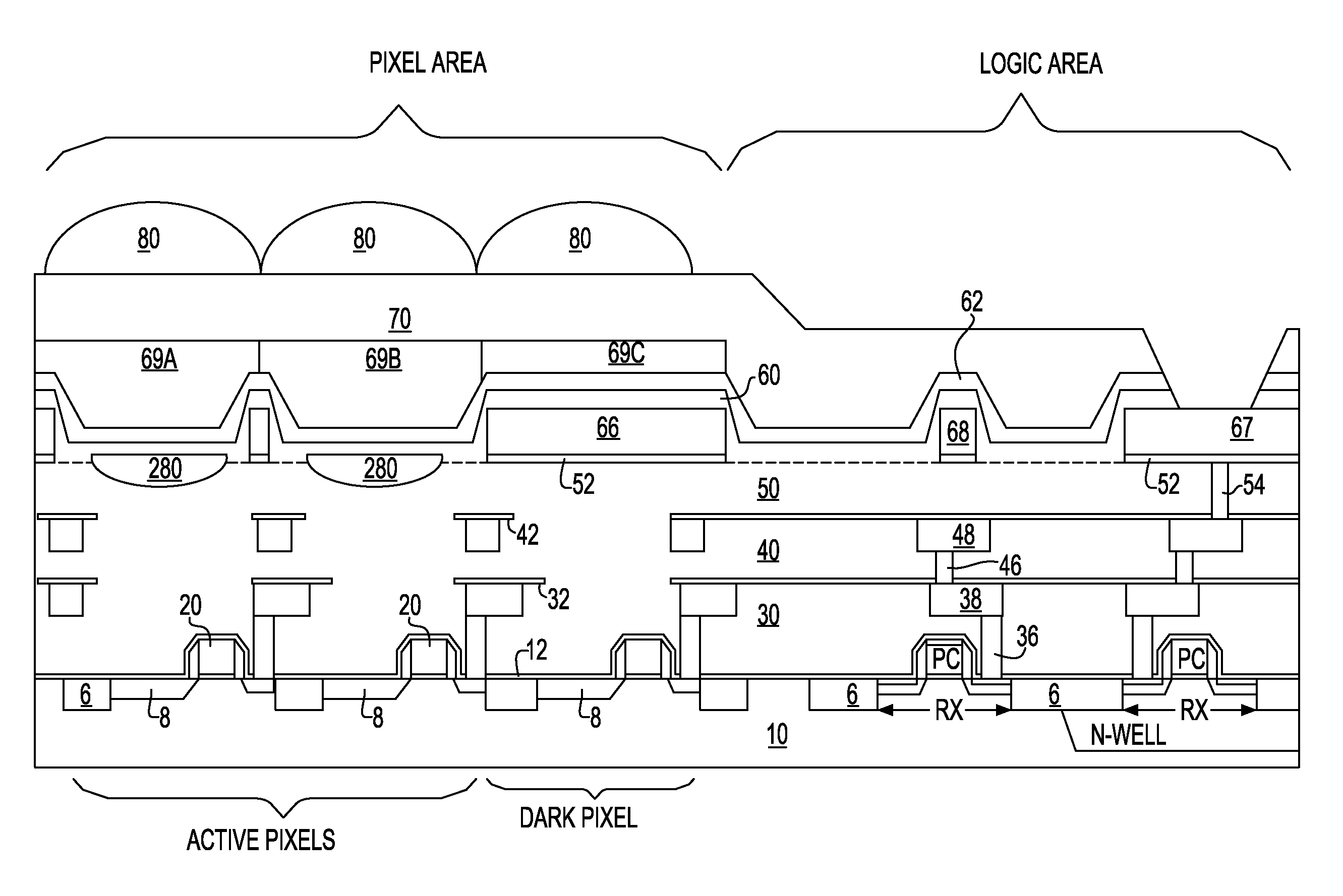
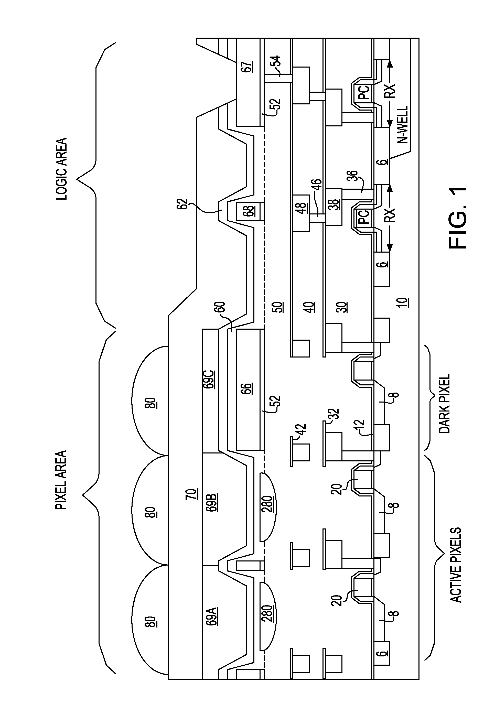
[0060]As stated above, the present invention relates to a method of forming an inverted lens that may be advantageously employed in a complementary metal oxide semiconductor (CMOS) image sensor structure formed on a semiconductor substrate, and structures formed by the same, which are now described in detail with accompanying figures. It is noted that like and corresponding elements are referred to by like names or reference numerals in the figures.

[0061]FIG. 1 shows a vertical cross-sectional view of an exemplary CMOS image sensor unit cell comprising a semiconductor substrate 10, gate electrode structures 20, a contact array and first metal line (CA-M1) level dielectric layer 30, a second metal line (M2) level dielectric layer 40, a second via (V2) level dielectric layer 50, a third metal line (M3) level dielectric layer 60, and a dielectric passivation layer 70. The exemplary CMOS image sensor unit further comprises pixel area which contain one pixel of each type and a logic area...


PUM


Abstract

A flat-top convex-bottom lower lens is formed by first applying a positive tone photoresist over a silicon oxide layer and an optional metallic barrier layer thereupon in a back-end-of-line (BEOL) metallization structure. The positive tone photoresist is exposed under defocused illumination conditions and/or employing a half-tone mask so that a cross-sectional profile of the positive tone photoresist after exposure contains a continuous and smooth concave profile, which is transferred into the underlying silicon oxide layer to form a concave cavity therein. After removing the photoresist, the cavity is filled with a high refractive index material such as silicon nitride, and planarized to form a flat-top convex-bottom lower lens. Various aluminum metal structures, a color filter, and a convex-top flat-bottom upper lens are thereafter formed so that the upper lens and the lower lens constitute a composite lens system.

Description

FIELD OF THE INVENTION[0001]The present invention relates to a method of forming a semiconductor structure, and particularly to a method of forming an inverted lens that may be advantageously employed in a complementary metal oxide semiconductor (CMOS) image sensor structure formed on a semiconductor substrate, and structures formed by the same.BACKGROUND OF THE INVENTION[0002]An image sensor converts a visual image to digital data that may be represented by a picture. The image sensor comprises an array of pixels, which are unit devices for the conversion of the visual image into digital data. Digital cameras and optical imaging devices employ an image sensor. Image sensors include charge-coupled devices (CCDs) or complementary metal oxide semiconductor (CMOS) image sensors.[0003]While CMOS image sensors have been more recently developed compared to the CCDs, CMOS image sensors provide an advantage of lower power consumption, smaller size, and faster data processing than CCDs as we...

Claims


Application Information

Patent Timeline
IPC IPC(8): H01L31/0232H01L31/18
CPCH01L27/14609H01L27/14685H01L27/14627H01L27/14621
Inventor BARRETT, TERENCEGAMBINO, JEFFREY P.LEIDY, ROBERT K.
Owner IBM CORP
Why Eureka
Try Eureka