Complementary metal-oxide-semiconductor device with embedded stressor

a metal-oxide-semiconductor and stressor technology, applied in the field of integrated circuits, can solve the problems of reducing short channel control, introducing other complications, and affecting the performance of transistors

Inactive Publication Date: 2009-10-01
IBM CORP +2
View PDF12 Cites 16 Cited by
  • Summary
  • Abstract
  • Description
  • Claims
  • Application Information

AI Technical Summary

Problems solved by technology

Use of the SiGe stressor, however, introduces other complications.
However, if the stressor is positioned too close to the gate, it becomes necessary to remove at least some of the halo implant region in the silicon channel.
The removal of even a portion of the halo implant region results in degraded transistor performance and short channel control, as boron dopants in the stressor diffuse into the silicon channel.
This further results in defects and dislocations due to crystal lattice mismatch between the SiGe stressor and the silicon channel.
Excessive defects result in transistor device leakage and degraded device performance.

Method used


Image

  • Complementary metal-oxide-semiconductor device with embedded stressor
  • Complementary metal-oxide-semiconductor device with embedded stressor
  • Complementary metal-oxide-semiconductor device with embedded stressor

Examples


Embodiment Construction

[0010]In one embodiment, the present invention is a complementary metal-oxide-semiconductor device with an embedded stressor. Embodiments of the present invention improve the germanium content of the SiGe stressor in a pFET while preserving halo regions. Embodiments of the present invention may be further applied to silicon carbide (SiC) material used in nFETs.

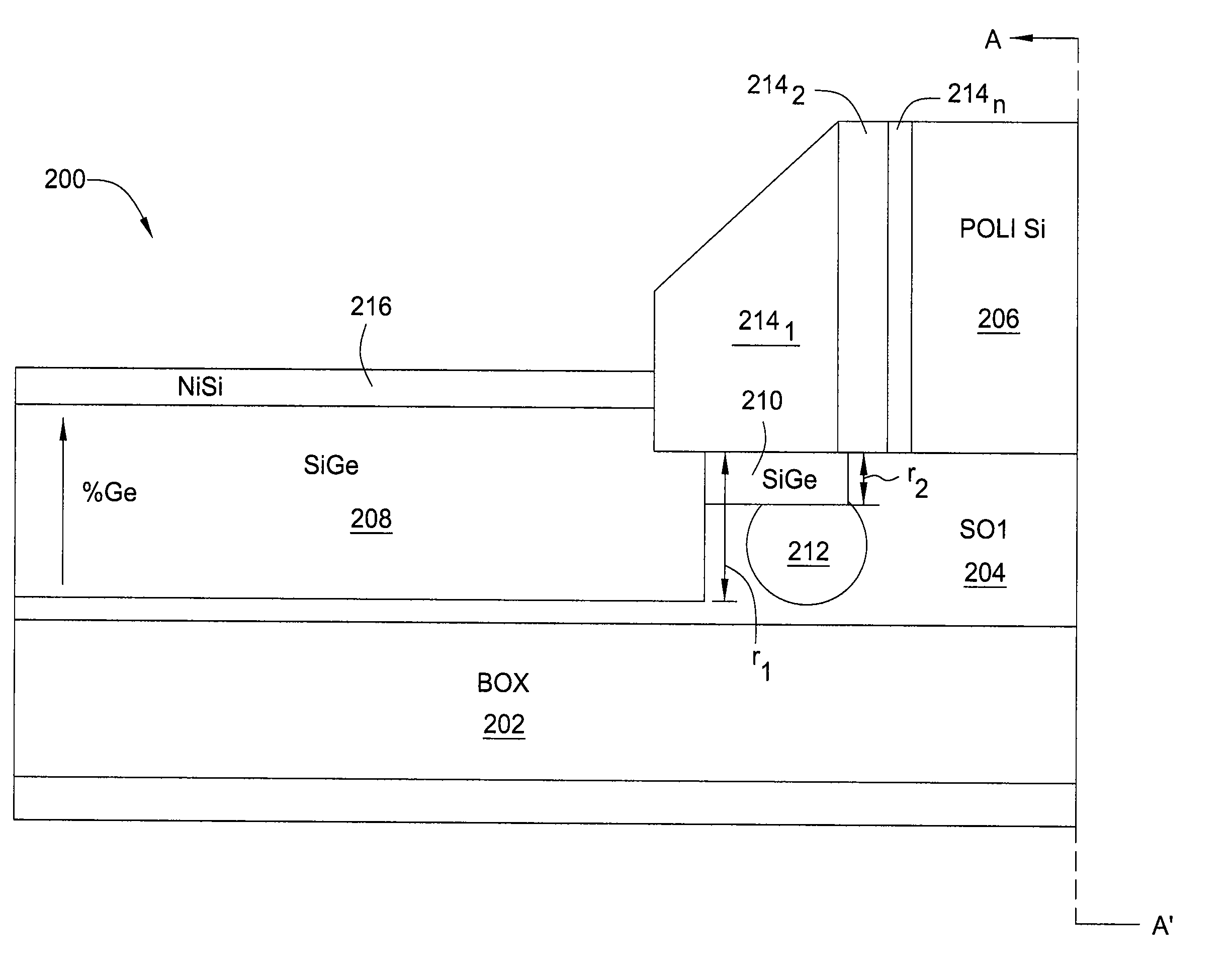
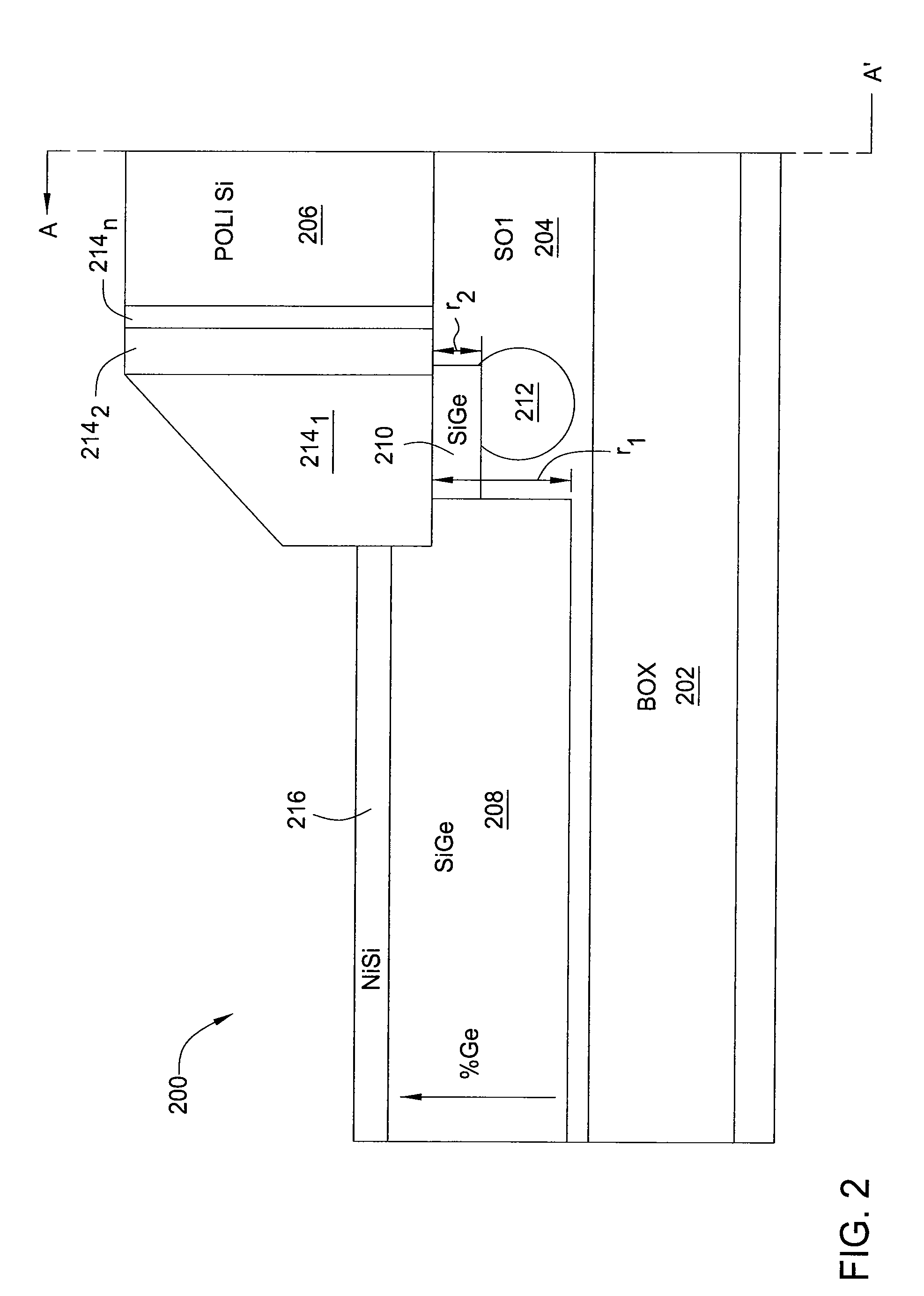
[0011]FIG. 2 is a schematic diagram illustrating one embodiment of a pFET 200 with an embedded stressor, according to the present invention. Specifically, FIG. 2 illustrates one half of the pFET 200, which has been cut along line A-A′.

[0012]As illustrated, the pFET 200 comprises a buried oxide (BOX) layer 202, a silicon on insulator (SOI) channel 204 disposed over the buried oxide layer 202, and a gate electrode 206 disposed over the SOI channel 204.

[0013]The SOI channel 204 further includes an embedded stressor 208, an extension 210, and a halo region 212. The stressor 208 is embedded in the SOI channel and is positioned late...


PUM


Abstract

In one embodiment, the invention is a complementary metal-oxide-semiconductor device with an embedded stressor. One embodiment of a field effect transistor includes a silicon on insulator channel, a gate electrode coupled to the silicon on insulator channel, and a stressor embedded in the silicon on insulator channel and spaced laterally from the gate electrode, where the stressor is formed of a silicon germanide alloy whose germanium content gradually increases in one direction.

Description

BACKGROUND OF THE INVENTION[0001]The present invention relates generally to integrated circuits (ICs), and relates more particularly to complementary metal-oxide-semiconductor (CMOS) devices that make use of strain-induced effects.[0002]One of the most effective approaches to improving carrier mobility and transistor device current in CMOS devices makes use of strain-induced effects. For instance, employing a boron-doped silicon germanide alloy (SiGe) “stressor” in the source and drain region of a p-type field effect transistor (pFET) provides uniaxial compressive strain to the silicon channel. This strain has been shown to enhance the driving current (performance) of the pFET. The stressor is typically positioned in a recess outward of the silicon channel, where the source and drain would normally be located.[0003]Use of the SiGe stressor, however, introduces other complications. For instance, the closer the stressor is positioned to the edge of the gate of the pFET, the more stres...

Claims


Application Information

Patent Timeline
Patent Type & Authority Applications(United States)
IPC IPC(8): H01L29/78H01L21/336
CPCH01L29/165H01L29/665H01L29/6656H01L29/78687H01L29/7848H01L29/78621H01L29/66742
Inventor CHAN, KEVIN K.CHU, JACK O.HAN, JIN-PINGKANARSKY, THOMAS S.NG, HUNG Y.QUYANG, QIQINGPEI, GENSUNG, CHUN-YUNGUTOMO, HENRY K.WALLNER, THOMAS A.
Owner IBM CORP
Why Eureka
Try Eureka