Semiconductor device and method of manufacturing the same and semiconductor device mounting structure

a semiconductor device and mounting structure technology, applied in the direction of semiconductor devices, semiconductor/solid-state device details, electrical apparatus, etc., can solve the problems of reducing the reliability of electric connection, affecting the manufacturing yield of the whole semiconductor device, and damage to the semiconductor element, so as to reduce the size of the resultant structure

Inactive Publication Date: 2009-10-01
SHINKO ELECTRIC IND CO LTD
View PDF8 Cites 28 Cited by
  • Summary
  • Abstract
  • Description
  • Claims
  • Application Information

AI Technical Summary

Benefits of technology

[0008]Exemplary embodiments of the present invention provide a semiconductor device and a method of manufacturing the same and a semiconductor device mounting structure, capable of providing an electric connection between

Problems solved by technology

However, in the case of the mounting method of stacking only the semiconductor elements, it is feared that, since the electric connection portions such as the through electrodes, or the like are provided to the semiconductor elements, the semiconductor elemen

Method used


Image

  • Semiconductor device and method of manufacturing the same and semiconductor device mounting structure
  • Semiconductor device and method of manufacturing the same and semiconductor device mounting structure
  • Semiconductor device and method of manufacturing the same and semiconductor device mounting structure

Examples


Embodiment Construction

[0030]A semiconductor device and a method of manufacturing the same and a semiconductor device mounting structure according to the present invention will be explained with reference to the accompanying drawings hereinafter.

[0031](Method of Manufacturing Semiconductor Device)

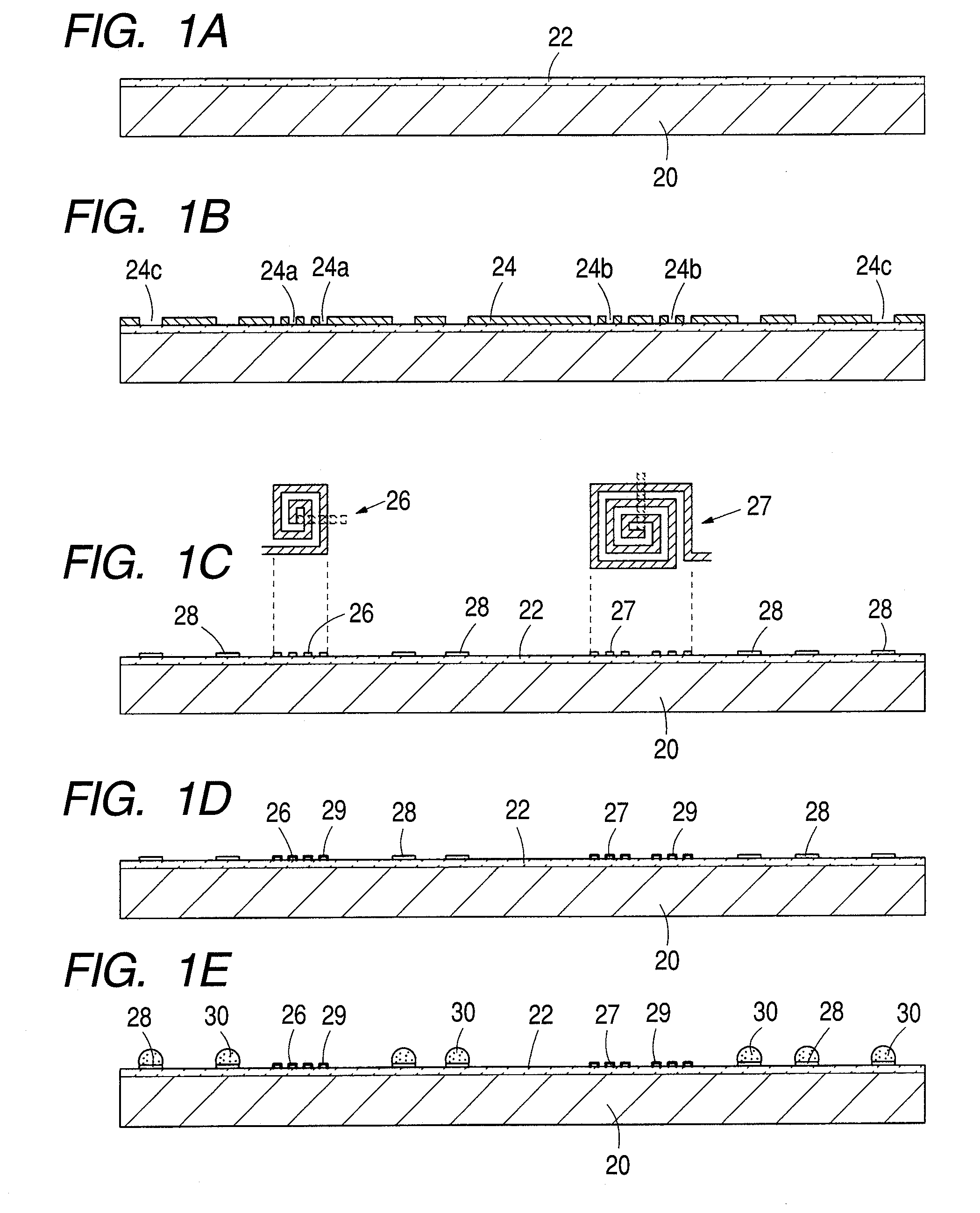
[0032]FIGS. 1A to 5B show a method of manufacturing a semiconductor device according to the present invention.

[0033]In the method of manufacturing the semiconductor device according to the present invention, predetermined processes are applied to a semiconductor wafer, and then the semiconductor wafer is diced into individual pieces as the semiconductor devices.

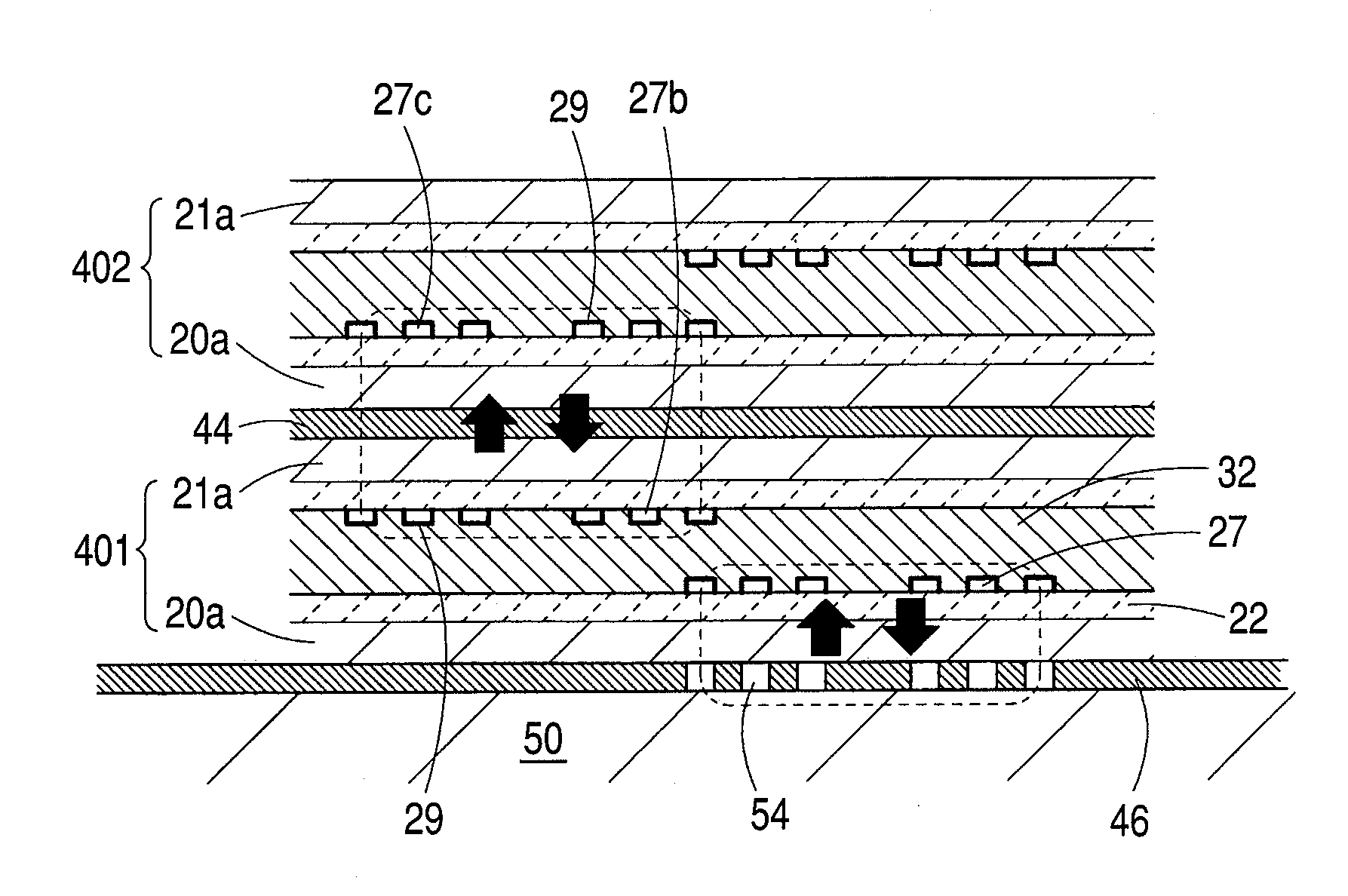
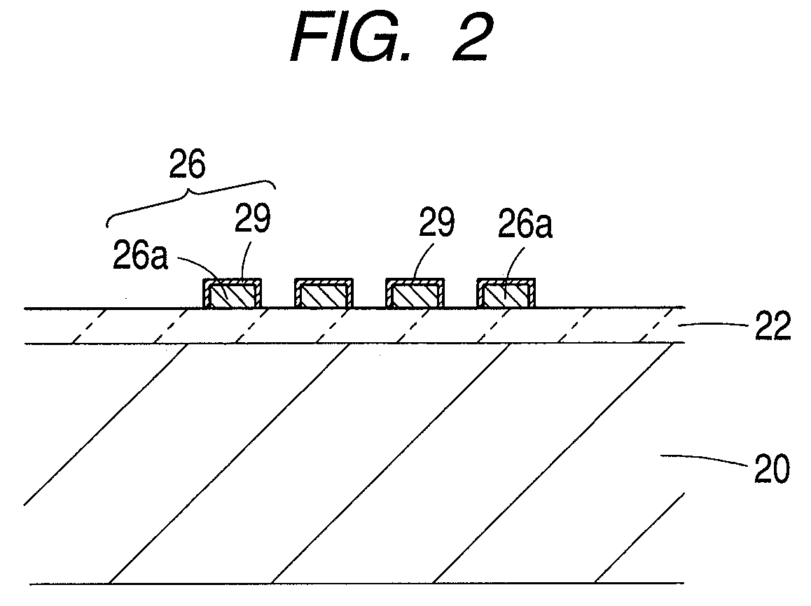
[0034]FIG. 1A is a sectional view showing of a wafer (semiconductor wafer) 20 on a surface of which devices are formed. A device layer 22 in which the devices are formed is provided on a surface (active surface) of the wafer 20.

[0035]FIG. 1B shows a state that a resist pattern 24 used to form wiring patterns for the electric connection and inductor pattern...


PUM


Abstract

In a semiconductor device that is formed by joining two semiconductor elements together to oppose device layers to each other, inductor patterns for transmitting and receiving a signal and feeding a power and bumps for connecting electrically the semiconductor elements and for supporting the inductor patterns and the semiconductor elements being arranged opposedly in an electrically isolated state are provided on a surface of the device layer of at least one of semiconductor elements and an electrically insulating material is filled in a space between opposing surfaces of the semiconductor elements.

Description

TECHNICAL FIELD[0001]The present disclosure relates to a semiconductor device and a method of manufacturing the same and a semiconductor device mounting structure. More particularly, the present disclosure relates to a semiconductor device having a structure in which a plurality of semiconductor elements are stacked and a method of manufacturing the same and a semiconductor device mounting structure.RELATED ART[0002]Out of the semiconductor devices in which semiconductor elements are mounted, the product in which a plurality of semiconductor elements are stacked has been provided to achieve a reduction in size and thickness of the semiconductor device.[0003]As the method of mounting the semiconductor elements in a stacked fashion, following methods can be considered. That is, (1) a mounting method of connecting the lower semiconductor element to the wiring substrate by the flip-chip bonding and then connecting an upper semiconductor element to the lower semiconductor element by the ...

Claims


Application Information

Patent Timeline
IPC IPC(8): H01L23/488H01L21/98
CPCH01L23/48H01L2225/06531H01L24/13H01L24/16H01L24/29H01L24/32H01L24/73H01L24/81H01L24/83H01L24/94H01L25/0657H01L25/105H01L2224/13144H01L2224/8121H01L2224/81815H01L2224/83101H01L2224/838H01L2224/94H01L2225/06513H01L2225/06541H01L2924/01029H01L2924/01078H01L2924/01079H01L2924/0781H01L2924/19042H01L2924/30107H01L23/645H01L2924/014H01L2924/01033H01L2924/01006H01L2924/01005H01L2224/81H01L2224/83H01L2224/05568H01L2224/05573H01L2924/00014H01L2224/05599
Inventor MASHINO, NAOHIRO
Owner SHINKO ELECTRIC IND CO LTD
Why Eureka
Try Eureka