Method and apparatus for imprinting microstructure and stamper therefor

a technology of microstructure and stamper, which is applied in the field of method and apparatus for imprinting microstructure and stamper therefor, can solve the problems of resin flow or inclusion of bubbles, dispersion of the thickness of the resulting printed pattern, and difficulty in achieving the effect of imprinting precision

Inactive Publication Date: 2009-10-01
HITACHI LTD
View PDF7 Cites 62 Cited by
  • Summary
  • Abstract
  • Description
  • Claims
  • Application Information

AI Technical Summary

Benefits of technology

[0011]A stamper made of flexible polymerizable film (resin stamper) disclosed in Japanese patent laid-open 2007-55235 is possible to be imprinted even if the member carrying the deformable layer has projections. This film is useful for increasing precision of imprinting. However, since the entire face of the resin stamper makes a contact with the entire face of the deformable layer from the beginnin

Problems solved by technology

As a area of the imprinting expands, there may be a local imbalance of a force applied to the pattern layer and the deformable layer, which leads to hindrance of resin flow or inclusion of bubbles.
However, since the entire face of the resin stampe

Method used


Image

  • Method and apparatus for imprinting microstructure and stamper therefor
  • Method and apparatus for imprinting microstructure and stamper therefor
  • Method and apparatus for imprinting microstructure and stamper therefor

Examples


embodiment 1

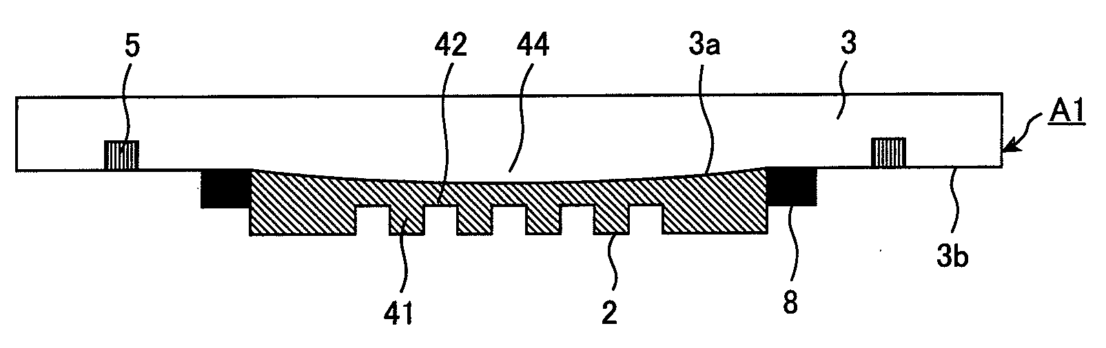
[0108]In this embodiment the stamper A2 shown in FIG. 1B and the imprinting apparatus shown in FIG. 3 were used to carry out imprinting the microstructure on the deformable layer.

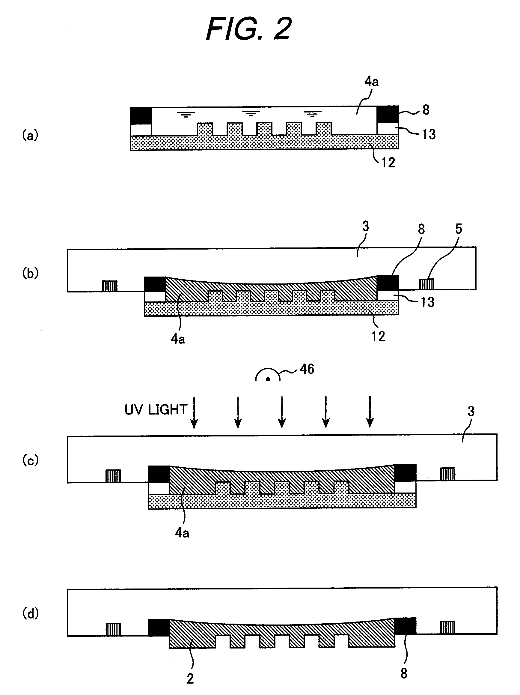
[0109]A method of manufacturing the stamper A2 is explained by reference to FIG. 2.

[0110]The original mold plate 12 was provided with a first frame 13 and the second frame 8 each being located to surround the periphery of the mold plate 12 so that a cavity is formed on the mold plate. The mold plate of single crystal had a diameter of 70 mm, a thickness of 0.5 mm. The mold pattern was formed by electron beam lithography. The formed patter was provided with grooves each having a width of 50 nm, depth of 80 nm with a pitch of 100 nm in a concentric relation.

[0111]The first frame 13 having an outer diameter of 75 mm, an inner diameter of 65 mm and height of 0.5 mm was fixed to the periphery of the original mold plate. The second frame 8 having an outer diameter of 75 mm, an inner diameter of 65 mm and a thickn...

embodiment 2

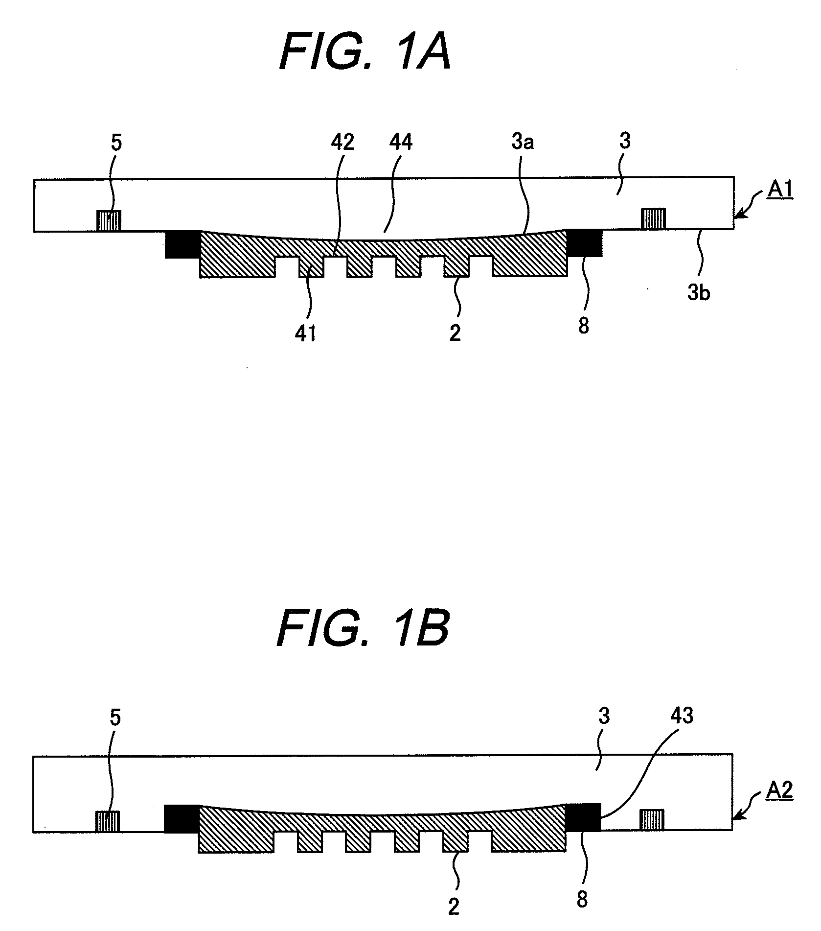
[0122]This embodiment will be explained by reference to figures. FIG. 6A shows a diagrammatic view of another embodiment of an imprinting apparatus of the present invention. In this embodiment the stamper was held by vacuum suction, while in embodiment 1 the pattern layer 2 was bonded to the substrate 3 with an adhesive. The stamper has a substrate having vacuum cavities, which are evacuated by a vacuum pump. The pattern layer 2 and the substrate 3 can be separated. The components of the imprinting apparatus are substantially the same as in FIG. 3A.

[0123]FIG. 6B shows a plan view of a substrate 9c having cavities 66, FIG. 6C shows a plan view of a plate 9a having vacuum suction ports 7a, 7b and FIG. 6D shows a plan view of a plate 9b having circular suction ports 7a, 7b.

[0124]FIG. 7 shows a process for manufacturing a pattern layer for a stamper shown in FIG. 6, wherein the pattern layer is not supported by a substrate 3. The original mold plate 12 made of silicon single crystal ha...

embodiment 3

[0134]Embodiment 3 will be explained in detail by reference to FIG. 8. In this embodiment the pattern layer differs from that of embodiment 2. The pattern layer consists of two kinds of resins 5a, 5b, which were laminated as shown in FIG. 8(b).

[0135]The resin layer 5b was made of polyurethane resin having a diameter of 65 mm and Yung's modulus of 10 MPa. The periphery of the resin plate 5b was surrounded by a frame 8 made of glass as shown in FIG. 8(a). The resin plate 5b was coated with photo-curable polyester resin 5a in dotted form as shown in FIG. 8(b).

[0136]An original mold plate 12 made of silicon single crystal having a diameter of 100 mm and a thickness of 0.5 mm was pressed down to the photo-curable resin coating on the resin plate 5b to expand the resin coating and imprint the pattern of the original pattern plate 12 as shown in FIG. 8(c). The original pattern was provided with a groove pattern each groove having a width of 50 nm, a depth of 80 nm and a pitch between the g...


PUM

PropertyMeasurementUnit
Microstructureaaaaaaaaaa
Transparencyaaaaaaaaaa
Modulusaaaaaaaaaa

Abstract

A method of imprinting a microstructure comprising: contacting a stamper comprising a pattern layer with the microstructure of the order of from micrometers to nanometers in one face of the pattern layer and a substrate supporting the pattern layer with an imprinting member having a deformable layer to which the microstructure is imprinted, wherein the pattern layer is supported on a round surface having a prescribed radius of curvature of the substrate, the center of the round surface protruding towards the rear face of the pattern layer; causing the deformable layer on the imprinting member; and separating the stamper from the cured deformable layer.

Description

CLAIM OF PRIORITY[0001]The present application claims priority from Japanese patent application serial No. 2008-89186, filed on Mar. 31, 2008, the content of which is hereby incorporated by reference into this application.FIELD OF THE INVENTION[0002]The present invention relates to a method of imprinting a microstructure of an order of micrometers to nanometers on an article, an apparatus for imprinting the microstructure and a stamper having the microstructure in a face thereof for imprinting the microstructure on the article. The microstructures may be classified into micrometer order structures and nanometer order structures.[0003]Recent years, microstructurization or shrinking of semiconductor integrated circuits are being in progress more and more. In order to realize micro-fine machining for the microstructurization, a high precision machining of pattern forming of the semiconductor integrated circuits has been conducted by using a photolithographic device. However, there may ...

Claims


Application Information

Patent Timeline
IPC IPC(8): G11B3/00B29C59/16
CPCB29C35/0888B29C37/0053B29C2035/0827G11B7/263B82Y10/00B82Y40/00G03F7/0002B29C2059/023
Inventor WASHIYA, RYUTAANDO, TAKASHIOGINO, MASAHIKOMIYAUCHI, AKIHIRO
Owner HITACHI LTD
Why Eureka
Try Eureka