Semiconductor device, manufacturing method of semiconductor device, display device, and manufacturing method of display device

a semiconductor device and manufacturing method technology, applied in the direction of transistors, instruments, optics, etc., can solve the problems of not being completely free of absorption, and achieve the effects of reducing the degree of absorption of visible light, ensuring stability, and ensuring stability

Active Publication Date: 2009-10-08
SAMSUNG DISPLAY CO LTD
View PDF4 Cites 42 Cited by
  • Summary
  • Abstract
  • Description
  • Claims
  • Application Information

AI Technical Summary

Benefits of technology

[0008]The present invention has been made in the above circumstances, and an object of the invention is therefore to provide a semiconductor device which can suppress generation of dark current and is suitably used as a current driving element of an organic EL device or the like as well as a manufacturing method of such a semiconductor device and a display device incorporating such a semiconductor device.
[0042]In semiconductor device according to the invention, the channel region of the semiconductor layer employs a polycrystalline film which is composed of the crystalline component and the non-crystalline component. Since the ratio of the crystalline component to the non-crystalline component is larger than or equal to 4, the degree of absorption of visible light is much lower than in ordinary amorphous IGZO films and no characteristic abnormality such as off-current increase occurs even under illumination with light. Therefore, the semiconductor device operates stably even if it has a configuration that the gate electrode, the pixel electrode, etc. are made of transparent materials and the channel region is caused to transmit light. As such, even when applied to a high-resolution transmission-type display or a bottom-emission-type light-emission display, the semiconductor device can provide a display in which a large aperture ratio is secured and high-quality display can be performed at a lower power consumption. Being a polycrystal, the semiconductor layer is advantageous over an amorphous film in terms of stability when the semiconductor device is used as a current driving element of an organic EL device.
[0043]The invention can provide a semiconductor device which can suppress generation of dark current and is suitably used as a current driving element of an organic EL device or the like as well as a manufacturing method of such a semiconductor device and a display device incorporating such a semiconductor device.

Problems solved by technology

However, in actuality, even conventional oxide semiconductors are not entirely free of absorptions in the visible range and are associated with a problem that, for example, an erroneous operation such as an off-current increase is caused by carrier excitation due to slight light absorption.
Its characteristics are influenced by a light source such as a backlight or an organic EL device so seriously as to be unsuitable for practical use.

Method used


Image

  • Semiconductor device, manufacturing method of semiconductor device, display device, and manufacturing method of display device
  • Semiconductor device, manufacturing method of semiconductor device, display device, and manufacturing method of display device
  • Semiconductor device, manufacturing method of semiconductor device, display device, and manufacturing method of display device

Examples


Embodiment Construction

[0048]An embodiment of the present invention will be hereinafter described in detail with reference to the drawings.

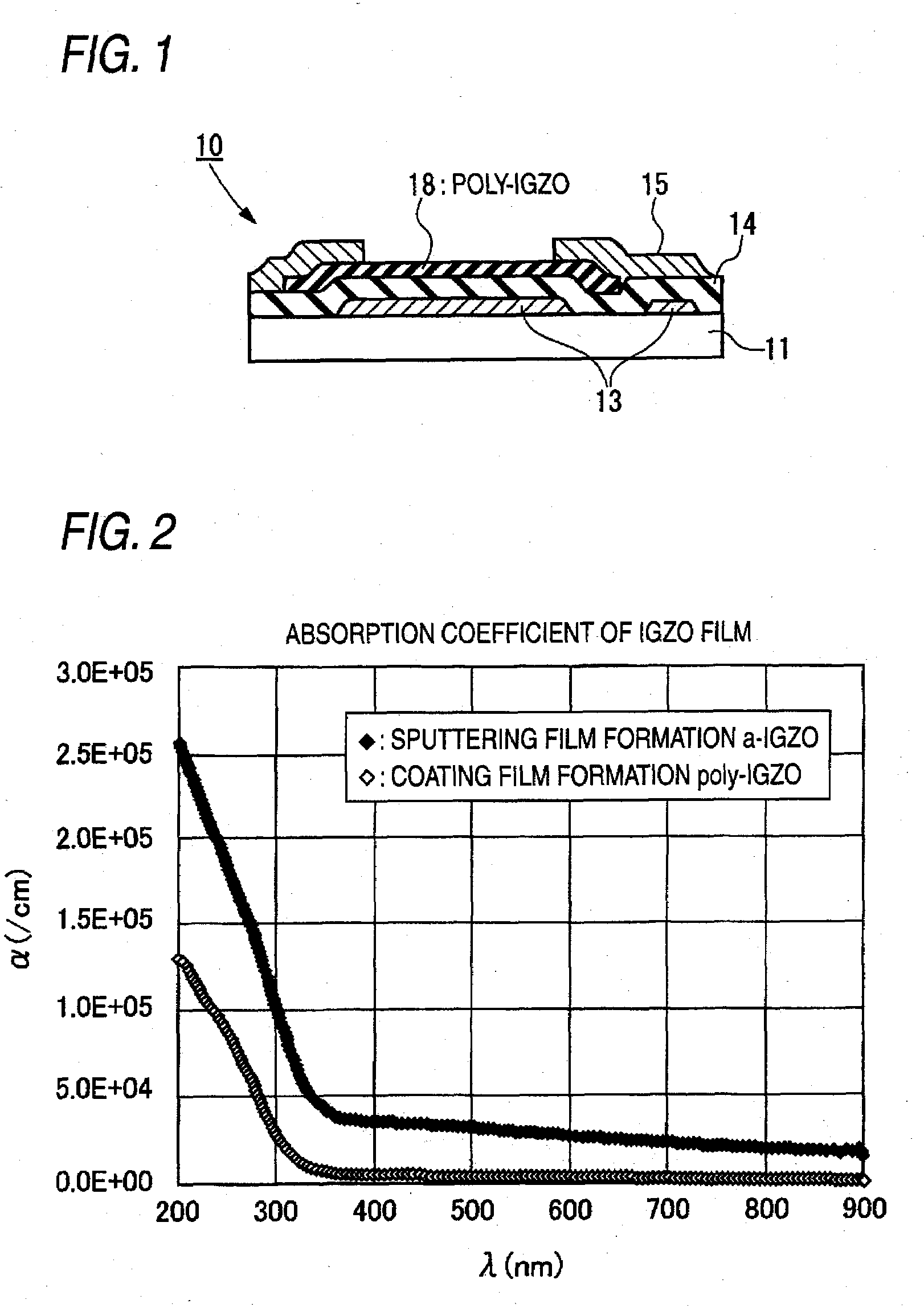
[0049]FIG. 1 is a sectional view showing an example basic configuration of a semiconductor device according to the invention.

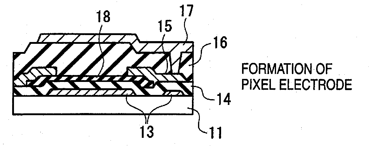
[0050]The semiconductor device 10 according to the embodiment serves as a semiconductor element having a TFT structure that is formed in each of plural pixel forming regions that are arranged in matrix form on a substrate such as a transparent glass substrate.

[0051]As shown in FIG. 1, the semiconductor device 10 is provided with a transparent substrate 11 and a gate electrode 13 is formed on the top surface of the substrate 11.

[0052]The substrate 11 may be a glass substrate, a quartz substrate, or a film made of PET, PEN, PES, or the like.

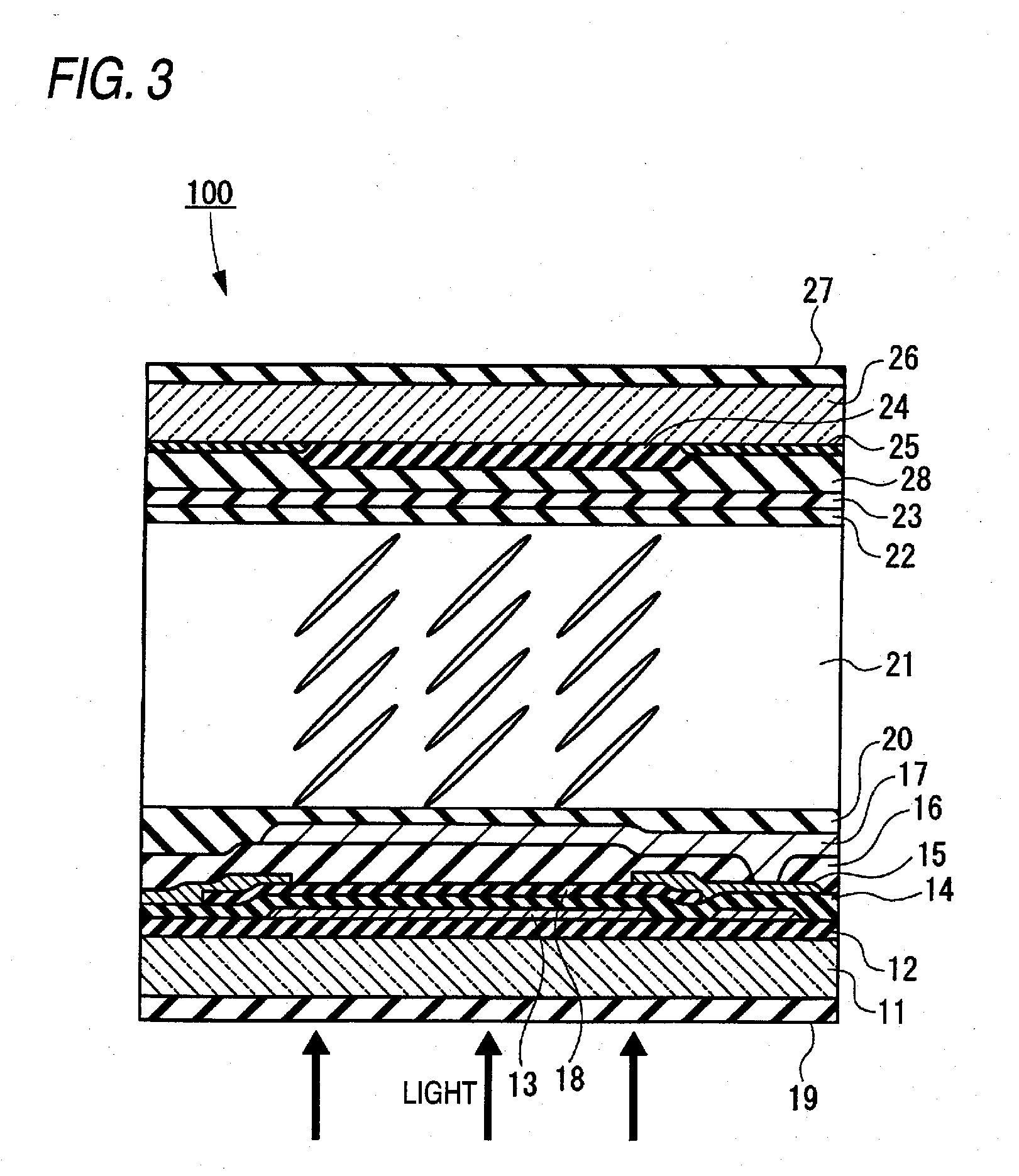
[0053]A transparent gate insulating film 14 made of SiO2, SiNx, Al2O3, Y2O3, or the like is formed on the substrate 11 so as to cover the gate electrode 13. A semiconductor layer 18 having an island-shaped patte...


PUM

PropertyMeasurementUnit
thicknessaaaaaaaaaa
wavelength rangeaaaaaaaaaa

Abstract

A semiconductor device includes a substrate and a semiconductor layer having a channel region, the channel region is made from an oxide semiconductor which satisfies Vc / Va>4 where Vc is a volume ratio of a crystalline component and Va is a volume ratio of a non-crystalline component.

Description

CROSS-REFERENCE TO RELATED APPLICATIONS[0001]This application claims the benefit of Japanese Patent Application JP 2008-098347, filed Apr. 4, 2008, the entire content of which is hereby incorporated by reference, the same as if set forth at length.FIELD OF THE INVENTION[0002]The present invention relates to a semiconductor device, a manufacturing method of a semiconductor device, and a display device. More particularly, the invention relates to a semiconductor device which is suitably used as a TFT (thin-film transistor) that is used as a switching element of each of pixels provided in an active-matrix-driven display panel.BACKGROUND OF THE INVENTION[0003]TFTs are used as switching elements of respective pixels in active-matrix-driven display panels as typified by LCDs. Although amorphous silicon is used most commonly as a semiconductor layer, its mobility is as low as about 0.5 cm2 / V·s. In view of this, in recent years, for use in large-size, high-resolution LCDs and organic light-...

Claims


Application Information

Patent Timeline
Patent Type & Authority Applications(United States)
IPC IPC(8): H01L29/786H01L33/00H01L21/02G02F1/1368H01L21/336H05B44/00
CPCH01L27/1225H01L29/7869H01L27/124
Inventor TANAKA, ATSUSHIUMEDA, KEN-ICHIHIGASHI, KOHEINANGU, MAKI
Owner SAMSUNG DISPLAY CO LTD
Why Eureka
Try Eureka